How Do I Flip and Rotate Components in Altium Designer and Other Schematic Functions

In this article, we'll give a brief overview of how to flip or mirror components in Altium Designer, as well as how to rotate components in different design documents. The functions in the schematic are slightly different than in the PCB layout, so follow along if you are a new user and want to learn these basic functions.
These functions can be accessed in multiple places: from the main menu at the top of the application window, using a hotkey, or using the Properties panel on the right side of the screen. After I show these points, I'll also outline some of the other basic functions in the schematics for placing and moving components as you work through a design. Without further delay, let's get started, and make sure you watch the video later in this article if you want further overview of the place and move functions in Altium Designer.

How Do I Rotate a Part in Altium Designer?
Parts can be rotated in both the schematic and the PCB layout. Note that a rotation in the schematic does not also rotate the component in the PCB layout, and vice versa. The options for rotation in each document are also different, as outlined below.
Rotating a Part in the Schematic and PCB Layout
Part rotation in schematics is limited to 90 degree increments. In the PCB layout, parts can be rotated in either 90 degree increments, or you can set an arbitrary rotation angle.
-
Use the Spacebar - The easiest way to rotate a part is to do this while it is flying on your mouse during placement. Go into the move command and then select the part. Once the part is flying on your cursor, use the “Spacebar” or the “Shift > Spacebar” to rotate the part one way or the other as shown in the pictures below.
-
Menu Option - Use the Edit > Move > Rotate Selection or Rotate Selection Clockwise pulldown menu and then click on the part to rotate it.
Either option will allow the part to be rotated as shown in the image below.
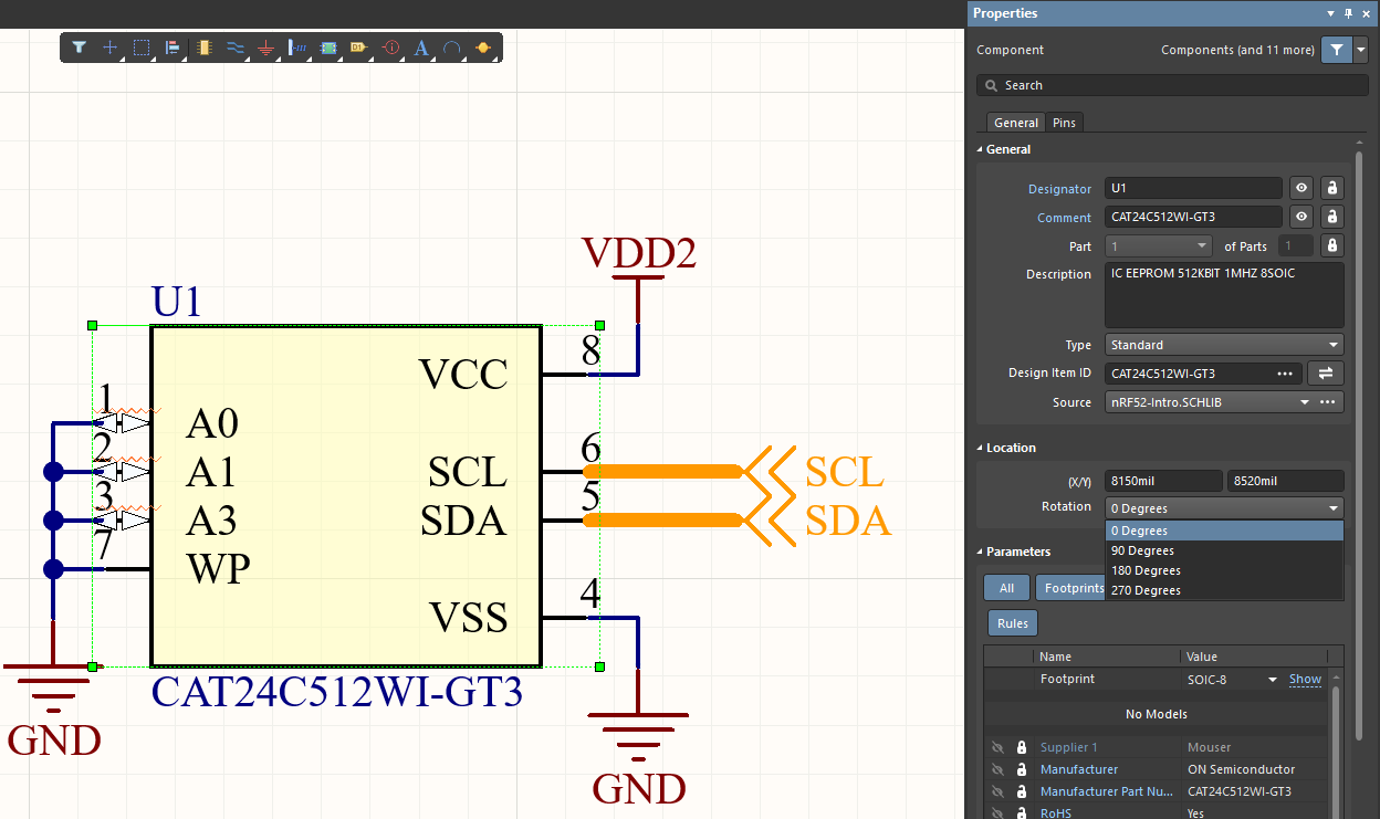
Rotating a component on the schematic
The other method for rotating the component is to use the Properties panel. To access the rotation setting, first open the Properties panel. Next, select the component you want to rotate. After selecting the target component, you will see a Rotation option in the Location area of the Properties panel.
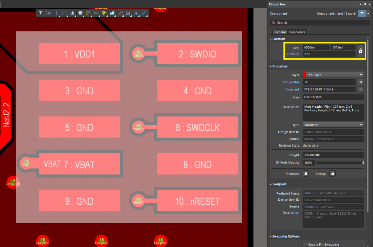
Once you have transferred the design into the PCB layout, you can rotate components with the same setting. Grab the component and press the Spacebar/Shift + Spacebar to rotate the component Counter clockwise or clockwise, respectively. Alternatively, you can use the Move --> Rotate Selection option from the top menu. There is also a Rotation entry in the Properties panel under the Location section (see below).
Note that the Spacebar/Shift + Spacebar hotkey will only rotate components in 90 degree increments, while the other options allow rotation to any angle. All positive angles are measured in the counter clockwise direction.
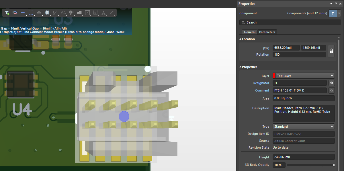
Components can also be rotated in 3D. To rotate a 3D model for a component, switch to 3D mode and select the model for the component in the PCB layout. You can then use the same features shown above to drag and rotate the component in 3D view, just like you would in the 2D view. You can also access the menu options to rotate the component in 3D, or you can select the component and use the Properties panel to rotate the component in 3D (see below).
Flipping/Mirroring a Component
When we refer to Altium flip component, we really mean creating a mirror image of the component. When you’re building your circuits, creating Altium mirror component in schematic editor is a great way to stay organized without crisscrossing multiple connections. Altium Designer provides a simple way to flip a component in the schematic.
As with the other commands, there are menu selections to Altium flip component. The easiest thing to do though is to use the “X” or “Y” keys while you are flying the part on your cursor to flip it either horizontally or vertically.
All of these commands to flip a component can also be done with multiple components. You can select and flip a group of components. While they are on your cursor, use the “X” or “Y” keys to flip them as you can see in the pictures below.
Using Altium, flip components as a group
Can Parts Be Mirrored in the PCB Layout?
Parts in the PCB layout can be mirrored in two ways:
- Flip a part to the other layer of the PCB
- Create a mirror image of a part on the same layer
To flip a component to the opposite layer of the PCB, select the component and drag it, and press the "L" key. The pads, silkscreen, and assembly information will appear on the opposite side of the PCB. Note that you could also use the Properties panel to set the layer for a component. For example, if you have a component on the top layer, and you set its location to the bottom layer, the result will be the same as if you were to use the "L" key.
While it is possible to use "X" and "Y" to mirror a component in the PCB layout, this is not recommended. If you do this in the PCB layout, it is equivalent to swapping the pad locations, which completely changes the PCB footprint for the component. If you select a component and try to do this mirroring, you will see the following warning.
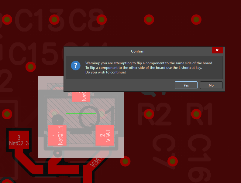
It is not recommended to use these keys to mirror the pad arrangement in the PCB layout. If you need to change the pad arrangement by mirroring, then it is best to change the footprint data for the component. To learn more about creating footprints, read this article.
Other Functions for Placement and Moving Components
Let’s assume that you’ve already created your project in Altium Designer and you’ve added a schematic. You should have also already set the schematic up for size and grids, as well as your preferences too. The next step is to add the components you want to use in your design.
These are all the basic steps of setting up your schematic for use. Altium Designer also gives you the ability to create symbols both manually and automatically. You can create these as single-part symbols or as multiple-part symbols. You also have the ability to pull components in from attached libraries or that you connect to through online services. Now that you’ve done all of this, you are ready to start working with the components of your design.
Placing Components
Rather than write out how to place components as you create a schematic and PCB layout, the video below explains how these basic functions work and where they can be accessed. Take a look at this video to learn more.
When placing a component you are going to be working from either the Explorer Panel or the Libraries Panel. The Explorer Panel allows you to connect to external libraries that are online to find parts. When working from the Explorer Panel you can hold your left mouse button down on the part in the Explorer Panel and then drag it over to the schematic sheet. You can also right-click on the part that you want and select “Place” as you can see in the picture below.
Selecting a component to place on the schematic in Altium Designer
When working from the Libraries Panel, you will be working with libraries that you have attached to your design. From here, you can also drag and drop the part from the Libraries Panel or right-click on the part and select “Place.” You can also select the part in the panel and then click the “Place” button at the top of the panel, or you can double-click on the part. Any of these actions will put the part on your cursor so that you can fly it into the design as shown below.
Flying the component in and placing it
While the part is flying on your cursor you can edit its properties by pressing the Tab key. This will allow you to change its values as you can see in the picture below where I have entered a new designator value. While editing the properties, the placement of the part will be paused until you use the Enter key to finalize your property changes.
Changing the value of the designator property
Once you have flown the part into position, click the mouse button or use the Enter key to place the part down on the sheet.
Selecting PCB Components in an Altium Designer Schematic
Once you have parts on the sheet, you may want to select them for other operations such as changing their properties or other edits. To select the part, click the left mouse button inside the part. You can also use the mouse to drag a rectangle around the part, but there are two different ways to select objects by dragging a rectangle.
By dragging your rectangle from the left to the right, you will only select those items that fall in the rectangle, while dragging your rectangle from the right to the left will select all objects that the rectangle touches.
This is extremely useful if you want to select just the designator of a part for editing. You would drag the rectangle from left to right so that it encompasses the designator but not all of the rest of the part. If you were to drag that same rectangle from right to left, the entire part would be selected.
Moving Components on a Schematic Sheet
To move a part that has been placed you can do the following:
-
Use the Edit > Move > Move pulldown menu and then click on the part to put it on your cursor as shown in the picture below.
-
Do the same command by pushing the “M” key twice (move > move), and then click on the part to put it on your cursor.
-
Hover your mouse over the part and hold the left mouse button down to put the part on your cursor. When you release the mouse button the part will place down at that location.
Moving a placed component
Copying Parts in Altium Designer
Another function in Altium Designer that is a great time-saver is to copy parts. You can take a part that is already on your design, like a resistor or a capacitor, and copy and paste it to create another instance of the same part. You can select the part and then go through the edit menu “Copy” and “Paste” commands. A much quicker way, however, is to use the standard copy-and-paste keyboard shortcuts “Ctrl-C” and “Ctrl-V,” just as you use in other applications. This command applies to any object in a schematic or PCB layout.
This is another point where we have to bring up PCB layout and schematic synchronization. While you can copy things like traces or vias in the PCB layout, you should not make copies of components in the PCB layout. This is because the corresponding symbol for a copied component will not appear in the schematic, and the design will not be synchronized. Instead, you should only copy parts inside the schematic, and then import that change into the PCB layout. This will ensure that your design documents always stay synchronized.
Altium Designer provides many shortcuts that notably improve your productivity. The shortcuts noted above were designed to help you work with components on your schematic more fluidly and effectively. Once you get into a pattern of using them, these shortcuts will save you a lot of time that you would usually spend on navigating through menus, you just need to use them.
Altium Designer has a proven history of regular upgrades and updates to make it the most efficient PCB design software available. If you would like to find out more about how Altium Designer can help you design your schematics more quickly and efficiently, feel free to talk to an expert at Altium Designer.

About Author
Related Resources


Related Technical Documentation


Table of Contents
- How Do I Rotate a Part in Altium Designer?
- Rotating a Part in the Schematic and PCB Layout
- Flipping/Mirroring a Component
- Can Parts Be Mirrored in the PCB Layout?
- Other Functions for Placement and Moving Components
- Placing Components
- Selecting PCB Components in an Altium Designer Schematic
- Moving Components on a Schematic Sheet
- Copying Parts in Altium Designer
Take advantage of the world's
most trusted PCB design system.
One interface. One data
model. Endless possibilities.
Effortlessly collaborate with
mechanical designers.
The world's most trusted
PCB design platform
Best in class interactive
routing
View License Options
Thank you, you are now subscribed to updates.