The Key Aspects Of PCB Specification Documentation

In all of our classes and consulting activities as well as the numerous articles we create, we always stress the importance of PCB documentation. Along with the PCB Fabrication Specification, this documentation is crucial to ensuring that a PCB is built right the first time and every time thereafter. Because the creation of this documentation occurs later during the design process, this step is given short shrift and/or not enough attention. When building complex, multilayer, high-density PCBs, it’s imperative that the appropriate documentation accompanies the PCB to the manufacturing phase of the project.
This article describes the various drawings, files and fabrication notes that must accompany every PCB that goes into fabrication.
The Customers and What They Should Receive
The PCB design process has three main customers:
- The PCB fabricator.
- The PCB assembler.
- The production test organization.
Each of the preceding customers requires data that is extracted from the design database and printed in a format that is applicable to their particular equipment. There’s also a need to create a document set that contains the design rules and data that is pertinent to each PCB design. The types of documents and their contents that are distributed include:
- The fabrication drawing and the recorded fabrication data.
- The set of design files used to create the film and other fabrication tooling information (sometimes referred to as the Gerber data).
- The assembly drawing and the necessary assembly information.
- The set of assembly files along with the bill of material and pick and place information.
- The set of test points that will be used by test engineering to prepare the needed test fixtures.
Additional information regarding the foregoing items is described below. It should be noted that the following list also includes the engineering drawing, but it is retained in house. It’s an important part of the process, so it is described below.
The Engineering Drawing
The engineering drawing looks much like a fabrication drawing except that it contains design information rather than fabrication information. As noted above, this document is retained in house and is not sent to the fabricator. The source for this drawing is the outline drawing that defines the size and shape of the PCB. The information recorded on this drawing comprises:
- The drill table, including the drill sizes and estimated quantity needed.
- The PCB stackup.
- The list of fabrication notes.
- The technology table that defines the routing rules.
- The list of all of the design files that must be prepared for the fabricator.
- The PCB outline drawing.
- A table that depicts the power supply voltages that will be assigned to each power layer of the PCB.
- Other appropriate, appurtenant notes.
The Fabrication Drawing
The fabrication drawing is derived from the above-noted engineering drawing. The final hole count is added to it, and the technology table is removed. The final PCB layer 1 is added to the outline drawing. Note: In the past, a drawing showing the location and size of all the drilled holes was drawn on this drawing. Fabricators no longer use this information and it has lost its value. The layer 1 artwork depicts how the finished PCB should look and is used instead.
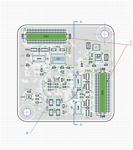
The fabrication drawing contains the stackup and shows each PCB layer by name, along with the Geber data per layer. One problem that occurs is that the information between these two sources is not the same. This can create problems for the fabricator who tries to match the design files with the layers in the stackup. The result is layers being stacked in the wrong order. Therefore, the same labels must be used for the design files as well as the names on the stackup drawing. Figure 1 shows how a fabrication drawing is laid out.

Figure 2. Layout of a Typical Fabrication Drawing
Table 1 is the list of fabrication notes that are required to build a high layer count and controlled-impedance PCB.

Table 1. A Typical Set of Fabrication Notes
Table 2 contains the list of design files required to fabricate a multilayer PCB.

Table 2. A List of Design Files Required by a Fabricator
Appended to the CAD net list, which is designated as IPC-356, are the X-Y location of all the component pins. The CAD net list is used in the preparation of the bare board test fixture, which is then compared to the net list that has been synthesized from the Gerber data.
The Assembly Drawing
The assembly drawing contains the information needed for assembling all of the electronic components to the PCB. It also contains information on how to attach all of the mechanical parts. Given the breadth of information contained within the assembly information, it is often several pages in length.
The Assembly Files
The assembly files contain the X-Y location of all the components; the bill of material; the code to be loaded into the programmable parts along with any other information needed by manufacturing to assemble the PCB.
The Test Point Files
The test point files are the list of test points that have been designed into the PCB to provide in-circuit test access to the PCB.
Summary
The documentation that is created to accompany the designed PCB into fabrication may seem very straightforward and may even be seen as a “no brainer.” But, it’s for these reasons that care be taken in creating this information. It’s also recommended that all of the various pieces of documentation, which is accumulated across the several design operations that go into creating a PCB are thoroughly reviewed and approved before they accompany the PCB on its way to final product realization.
If you want to know more, why not browse our product page for a more in-depth feature description or call an expert at Altium.


