


Best Practices for DNI/DNP Components in Your PCB BOM

At a Glance
You can use the DNI/DNP designation on components in your PCB BOM to create design variants as long as you’ve created your layout correctly.


If you’ve ever looked at the BOM for a reference design or an open-source project, you may have seen a comment in some of the entries in your BOM. This comment is either “DNP” (do not populate) or “DNI” (do not include). These entries are used to tell your PCB assembler “the bare board was designed to mount these components, but please do not include these parts in the final PCB assembly.”
If you think about it, every component placed in the PCB requires some level of placement and routing effort, which takes time (and money if you’re working for a client). Depending on the component count in the board, you could potentially have dozens of components marked DNI or DNP in the BOM. This begs the question, why would anyone design a board with components they don’t plan to include in the final assembly?
If you’ve never run into a situation where you need to mark a BOM entry DNP, you’ll quickly find some situations if you need to build a test board or swap out a component for a variant. Let’s look at these two areas as they are the most common instances where you will need DNI/DNP components.
Two Ways to Use DNI/DNP Components
There are two popular reasons a DNI or DNP component are used in a design: to accommodate variants of a component, or to accommodate different configurations on components. Both of these cases apply when components have variants with additional features on reserved pins (this is common on large ICs), or when a component has multiple configuration pins, and you want to accommodate different configurations without changing your layout.
Accommodating Component Variants and Upgrades
Not all components have drop-in replacements, but those that do may have some additional features that require placing or omitting an external component. Consider two MCUs from the same product line: one has on-chip Flash and SRAM (variant A), while the other only has SRAM (variant B) and requires an external Flash chip. If you want to use this MCU, you would design the board to support variant B and include the external Flash module. If you can get stock of variant B, you can place it and DNP the Flash module.
The advantage of doing this is in terms of convenience: you only need to design one board, but it could be used with multiple variants of a specific component or circuit. To switch up to a new variant, just make sure to review the BOM and add/remove entries as necessary.

Doing this requires considering two important points. First, the package sizes and land patterns on your high-end vs. low-end component need to match. Second, the pinouts for the dedicated pins have to match. This is typically done on larger processors, where a low-end variant of a component will just have some features on the chip disabled. This practice is useful because it gives you a backup option for a component in case your first choice is out of stock.
The other option is to create a reconfigurable design, which might mean you can avoid all this business with marking DNI/DNP components in your BOM.
Making a Reconfigurable Design
If you look at some components, specifically MCUs/FPGAs or other large ICs, they will have configuration pins that need to be connected to power or ground, often through a resistor or another passive component. This isn’t limited to large processors; low-pin count components like power regulators or ASICs can have some configuration features that are toggled by placing a resistor to VCC/VDD or to GND. A design with one of these components can be made reconfigurable by DNP-ing certain configuration resistors.
This is a good way to create a single board that can be manufactured in multiple runs, and the configuration is changed by simply placing or DNP-ing various configuration resistors. To create this type of board, you have to first select the right configuration resistors according to your component datasheets. There are a couple ways to do this:
- Always place all configuration components, even if they are not needed, and place a 0 Ohm resistor in series with each configuration component. You can then close or open that connection by placing/DNP-ing the component as needed.
- DNP various configuration components directly, but always leave copper connecting directly back to the target component.
If you’re not in the mood to mark DNP components, you can use a 2-pin jumper to bridge to open a connection between a configuration pin and PWR/GND, or to open/close the connection between a configuration passive and a pin. In this case, it’s best to just place all possible configuration components you might need, and then use jumpers to enable/disable connections with these components. This is a common practice with development boards and evaluation kits.

Placing 0 Ohm resistors and jumpers has saved me more times than I care to remember. In my opinion, jumpers are the best choice for controlling DC configuration settings as they can also act like a simple test point. You can probe these with a multimeter if needed during board bring-up just to check that you’re getting the test results you would expect.
Obviously, these are not the only ways to use the DNI/DNP component designation, but it should give some context as to why this is used in schematics and in a PCB layout. A more elaborate method that can be used beyond manually marking DNI and DNP in your schematics/bill of materials is to use a design variants management feature.
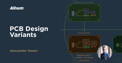
Design Variants
A more sophisticated approach is to use design variants to create variations on a basic design, which might include assigning DNI/DNP status to certain components. Design variants start with a base design that includes everything required to build the board. Once a variant is created, the variant could have certain components added or swapped, or it could have a component marked DNI/DNP. These changes are also imported into the PCB layout, meaning each schematic variant also has a PCB layout variant. By starting with a base design and creating variants, you can eliminate some of the ambiguity that arises when manually annotating BOM and keeping track of separate file groups.

Once you’ve finished your PCB layout and designated required DNI/DNP components in your schematics or created your variants, you can quickly export your BOM and other manufacturing files using Altium. Users can manage component placements in their schematics, DNP components, manually annotate the BOM, or create variants. They can upload and store design data in the cloud, and easily view projects via a web browser in a secure platform.

About Author
Related Resources
Related Technical Documentation
Table of Contents
Design to Release, Without the Friction
- Keep reviews tied to the right version
- Reduce handoff confusion and rework
- Spot sourcing and release risk earlier
- Work solo, share when needed
Get Started
Thank you, you are now subscribed to updates.

