


Demonstrations for Multi-Layer PCB Designs: Best Uses for Each Layer


Your PCB layers are the key to success in your design, but the placement of layers and assignments of layer type can make the difference between success and failure. It's not just about determining where to route things; how you arrange layers in the stack will determine whether noise issues compromise your design. Layer arrangements can make the difference between proper functionality or failure, as well as whether a design can pass EMC testing and be put into mass production.
If you're a new designer getting into your first multi-layer board, or you suspect your routing approach is leading to circuit failure, these layer selection and assignment guidelines are for you. The principles here are well understood by high-speed digital designers and RF designers, as well as EMC experts who specialize in debugging PCB layouts.
Signal or Plane?
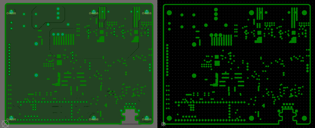
PCB design software allows selection of two types of layers: signal layers and plane layers. Technically, a signal layer can be used as a plane layer simply by filling it with copper, but a plane layer cannot be converted to a signal layer. The main difference between these two layer types is how they are displayed in your PCB editor and in a Gerber file. PCB editors and Gerber viewers display plane layers in negative, where the lines in the image show where copper is being removed from the layer.
Plane layer in the PCB editor (left) and the same plane layer shown in the CAMtastic Gerber viewer (right).
When building a stack-up, your job is to arrange these layer types in your PCB. In most PCBs, a uniform copper ground layer is required, whether it is defined as a signal layer or plane layer in your PCB design software.
Where to Place All the Plane Layers
Since a plane layer will be needed in most cases, where should you start placing planes in your PCB stack-up? The answer depends on the number of layers in the stack-up, as each layer in a stack-up provides certain functions related to routing, signal integrity, and EMI. We can find very good guidelines in two-layer and four-layer boards, extending to six or more layers.
Two-Layer Boards
In a two-layer PCB, you have to do all of your routing on the top and bottom layers. It is almost always the case that you will be routing on both sides of the board, so you will not have complete planes.
Although you don't have a plane layer in your two-layer board, you can fill in the two-layer board with copper pour and connect it to the ground net. This gives you some level of definition for ground, which will aid suppression and reduce EMI susceptibility. It is also possible to route some high-speed interfaces on a two-layer board using grounded copper pour, as I have demonstrated in another article on routing USB in two-layer PCBs.
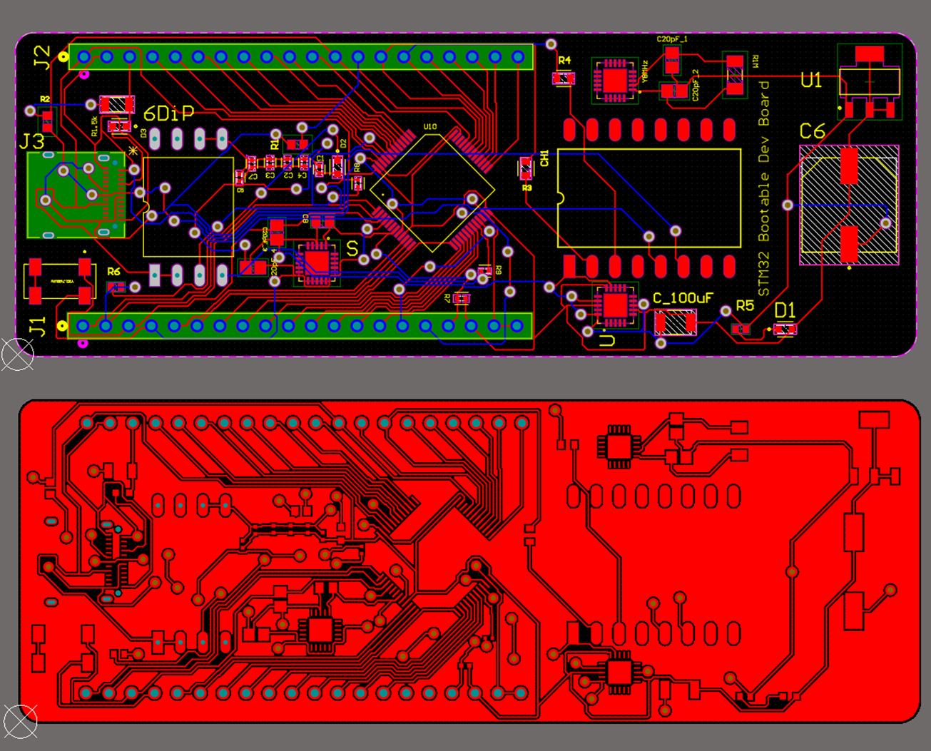
Two-layer PCB (top) and the same PCB with copper fill to define ground (bottom). As long as the component density is not too high, and there are no high-speed interfaces in the design, then the use of copper pour as a substitute for a ground plane can be acceptable.
The image above shows an example where grounded copper pour is sufficient to fill in gaps and provide a significant amount of ground throughout the PCB, functioning much like a plane. When the density of component placement gets very high, or when you have many high-speed interfaces, two-layer boards are no longer appropriate due to the difficulty in defining ground, and you must use a four-layer board with planes.
Four-Layer Stack-Ups
Four-layer PCBs are entry-level stack-ups for high-speed PCB design, and they work best with at least one plane layer. Ideally, you should have two internal plane layers. This provides the best option for EMC performance while also addressing a critical part of high-speed design: defining impedance.
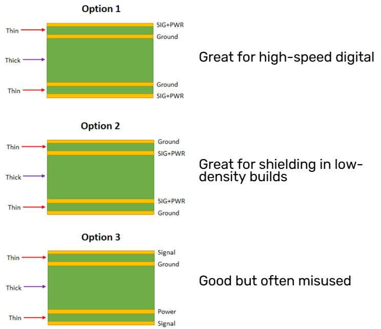
The most common uses of four-layer stack-ups are shown in the images below. Each of these stack-ups uses planes in some way. Note that only one of these stack-ups uses a power plane, or possibly a single power layer with multiple rails.
The simplest recommendations that aid signal integrity and EMI/EMC are:
- Place the ground layer adjacent to the highest speed signals.
- Do not route high-speed signals over splits in any ground polygons or power polygons.
The second recommendation is a nod to the structure of the third stack-up with the power layer, as the power layer could consist of two or more large rails at different voltages. Finally, the signal layers are placed above uniform ground, allowing for any density of components without removing too much copper from the surface layers.
Six or More Layers
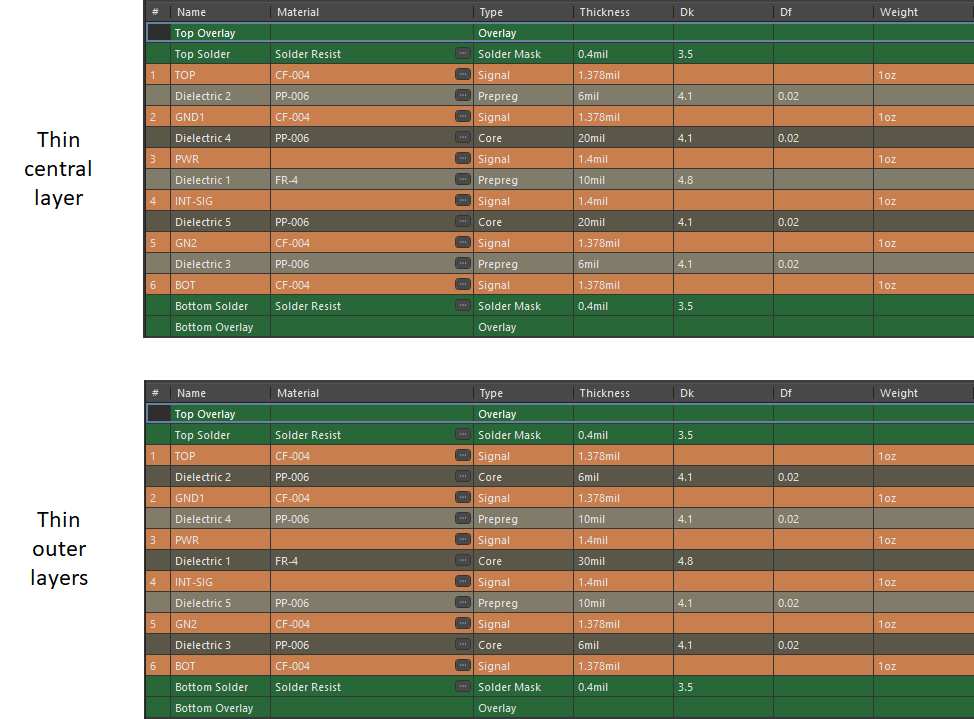
Going beyond four layers is normally done because controlled impedance is needed on more than two layers. With six-layer stack-ups, the best approach for the internal layers is to assign one of these as a signal layer, while the outer four layers are signal/ground pairs.
The image on the bottom with the two thin outer layers works allows for two internal signal layers, but it is best if these internal signal layers don't carry very high-speed signals. This is much less common than the layer arrangements with a dedicated power layer, which is superior for digital PCBs from both power integrity and signal integrity perspectives.
On the right, the power layer is normally not a plane; it is a signal layer used for large copper rails at different voltages. Essentially, the power layer is filled with copper for these big rails. When a power plane is needed, it is usually for the convenience of routing power to the components, or when the power plane must carry very high current.
To continue expanding beyond six layers, the best approach from an EMC perspective is to add a signal/ground pair into the six-layer stack-up. By doing this, you continue to shield the new signal layers with the added ground layer. Each ground layer could be added as a plane layer or as a signal layer filled with copper pour.
Configuring Each Layer for the Best Use in Your PCB Design
To start assigning layer types in Altium Designer, you can create a new PCB and open the Layer Stack Manager. A default layer selection will be shown in the Layer Stack Manager if you are starting from a brand new PCB. Note that you do not need to assign a board outline before assigning layer types; either step can be done first.
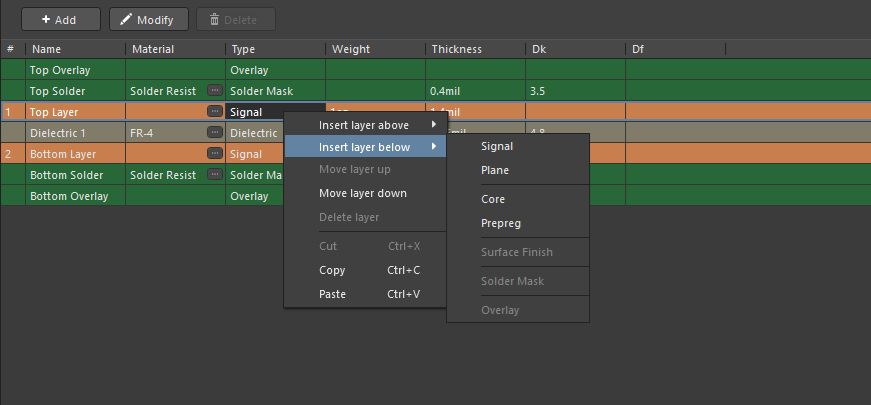
Inside the Layer Stack Manager, the default layer arrangement is shown below. Right-clicking on the existing layers will provide options to add new insulators or copper layers.
Select these menu options until you've added the desired number of layers. You can then go through and change the insulator thickness values and copper weight values in the layer stack.
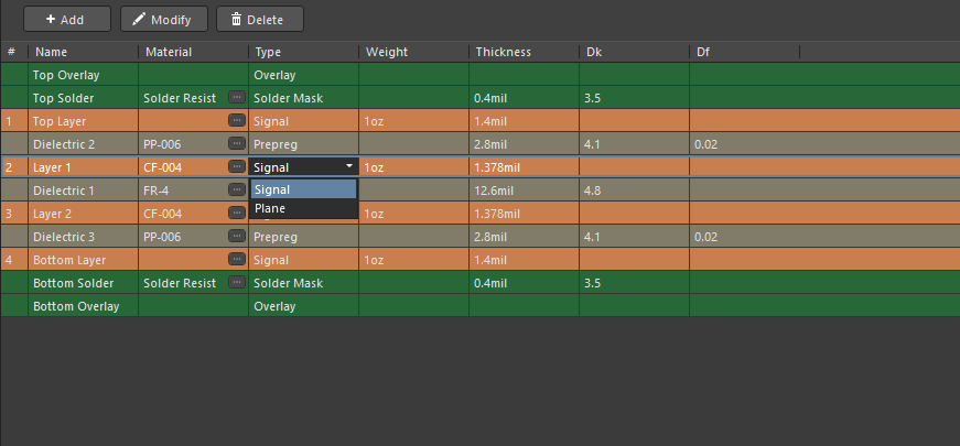
Next, you can assign different copper layers to Signal or Plane layer types. By default, as you add new copper layers, they will be added as signal layers. Select the drop-down menu on copper layer type and change it to a plane as needed.
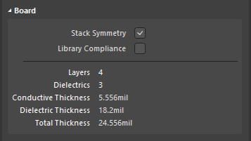
As new layers are added, you will notice that the Layer Stack Manager enforces stack symmetry by default. This means, for example, in a four-layer board, if you put a plane on layer 2, a plane will also appear on layer 3. This can be changed in the Properties panel by clicking the stack symmetry checkbox.
To learn more about the full capabilities of the Layer Stack Manager in Altium Designer, take a look at the documentation at this link.
Whether you need to build reliable power electronics or advanced digital systems, use the complete set of PCB design features and world-class CAD tools in Altium Designer®. To implement collaboration in today’s cross-disciplinary environment, innovative companies are using the Altium 365™ platform to easily share design data and put projects into manufacturing.
We have only scratched the surface of what’s possible with Altium Designer on Altium 365. Start your free trial of Altium Designer + Altium 365 today.

About Author
Related Resources
Table of Contents
Design to Release, Without the Friction
- Keep reviews tied to the right version
- Reduce handoff confusion and rework
- Spot sourcing and release risk earlier
- Work solo, share when needed
Get Started
Thank you, you are now subscribed to updates.

