


Precision PCB Design Software with a Differential Line Impedance Calculator


Altium Designer’s differential line impedance calculator will set up your impedance-controlled differential pair routing widths for you.
ALTIUM DESIGNER
For better impedance control, use PCB design software you can trust.
One thing is for sure: When you are routing a high-speed PCB design you are going to be working with impedance-controlled routing and differential pairs. There have been trace routing tools available for a long time that help with differential pair routing, and designers have had access to impedance calculators to determine their trace widths. But to find a PCB routing system that calculates trace widths automatically factoring dielectric constants and the board layer stackup, and then automatically inputs that into the design rules, is a little more difficult. Then on top of that, finding a PCB design tool that will automatically calculate differential pair trace widths based on impedance calculations is almost unheard of. That’s when the engineering team at Altium Designer went to work to make sure you’re covered.
The new enhanced layer stack manager in Altium Designer will do all of what you are looking for in high-speed impedance controlled routing, including calculating your diff pair widths. By entering your board layer stack materials from a premade materials library already equipped with information like dielectric constants, you can perform impedance calculations based on a number of routing profiles including stripline, microstrip, and differential pairs. That information is then made available to the design rules to set up the precise routing trace widths that your board needs. You will be hard pressed to find a PCB layout toolset that can help you more than Altium Designer can.
A Little More about Differential Pair Routing & Transmission Lines
Differential pair routing used to be a painful process of manually routing each trace of the pair tediously side-by-side to accomplish the task. Fortunately, differential pair routing tools have given designers the ability to easily route the pairs together while obeying a set of design rules that governs trace widths, spacing, and how far the transmission pairs can diverge from each other. Understanding why differential pairs need to be routed so precisely for proper signal transmission is important to the entire high-speed design process, and Altium Designer has provided some information here to help.
Understanding the Basics of Differential Pair Routing
Here is some basic information on what the purpose of differential pair routing is and how best to accomplish it.
- Here are some important differential routing tips and tricks.
Learn More about differential pair routing to preserve signal integrity.
- Inadequate PCB design software can leave out important features such as diff pair routers.
Learn More about how design software can help you with your differential pair routing.
- Proper low voltage differential signal routing can eliminate the crosstalk.
- Differential pair routing is one of many aspects of high-speed design.
Learn More about length tolerance matching and other high-speed design principles.

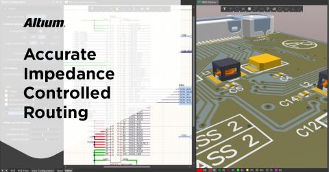
Setting up the impedance calculator for differential pairs in Altium Designer
Routing Diff Pairs with a Differential Line Impedance Calculator for Optimal Signal Transmission
With Altium Designer, you no longer have to use a separate calculator to determine your trace widths and then enter those values into the design rules. Instead, you set up your board layer stackup with materials and thicknesses, and then let the calculator input the correct trace widths into your design rules for the impedance values you have chosen. The next step is to do the same calculations for differential pairs, and the enhanced layer stack manager in Altium Designer will do just that. So put away your manual layer thickness, dielectric constant, and impedance calculations you’ve been using. Altium Designer can do the heavy lifting of differential pair impedance calculations for you from now on.
Altium Designer Does the Impedance Calculations Based on Your Layer Stack
With a handy library of board materials to choose from, Altium Designer will calculate your trace widths and thickness based on the impedance values that you need.
- Altium Designer’s new enhanced layer stack manager will allow you to calculate the impedance for multiple configurations including differential pair gaps.
Learn More about controlling differential pair impedance in Altium Designer’s layer stack manager.
- Altium Designer’s impedance calculator takes your board layer stackup information and sends the trace width and thickness results to your design rules.
Learn More about using the Altium Designer’s impedance calculator in this brief tutorial.
- Controlling the impedance in your design is dependent on the board layer stackup you choose.

Routing differential pairs in Altium Designer
High-Speed PCB Layout in Altium Designer
You’ve built the board layer stackup and prepared your design rules based on the trace width input from Altium Designer’s impedance calculator. But there’s a whole lot more to high-speed digital design than just that. Fortunately, the advanced technology that you’ve seen in the layer stack manager and impedance calculator is just the beginning of what Altium Designer has in store for you. Based on a 64-bit multi-threading platform, Altium Designer has all the power that you will need for your high-speed Printed Circuit Board designs.
Starting with component placement, Altium Designer has a multitude of different placement algorithms to help you locate and align your components the way that you need them to be. When it comes to trace routing you won’t find a more comprehensive set of routing tools than what’s available to you in Altium Designer. Whether it is interactive routing, auto-interactive routing, or auto-routing, Altium Designer’s intelligent routing tools will help you to complete your routing quicker and more efficiently than you would have thought possible. To ensure that your high-speed PCB is designed the way it needs to be, Altium Designer’s full array of high-speed design rules and constraints will give you control over measured lines, routing topologies, and signal paths. Together with a powerful schematic editor and automated manufacturing output tools, Altium Designer has everything you need to successfully complete your high-speed layout.
Powerful PCB Layout Tools to Get Your Job Done Right
There’s a lot to accomplish when working on a high-speed PCB design, and Altium Designer has all of your needs covered with its powerful set of design tools.
- Altium Designer’s component placement features will ensure that your components are placed exactly where you need them to be.
Learn More about smart component placement in Altium Designer.
- It all comes down to the routing and Altium Designer offers a vast array of intelligent routing tools to get the job done.
Learn More about intelligent interactive routing in Altium Designer.
- Measured lines, routing topologies, differential pair routing, and signal paths are all easily handled with Altium Designer’s high-speed design tools.
There’s a lot that will go into your high-speed design, and it starts with configuring the board layer stack in order for Altium Designer’s differential line impedance calculator to do its job. You’ve got the most amazing PCB design tools out there ready for you to use, so put Altium Designer to work for you today.

About Author
Related Resources
Related Technical Documentation
Table of Contents
- A Little More about Differential Pair Routing & Transmission Lines
- Understanding the Basics of Differential Pair Routing
- Routing Diff Pairs with a Differential Line Impedance Calculator for Optimal Signal Transmission
- Altium Designer Does the Impedance Calculations Based on Your Layer Stack
- High-Speed PCB Layout in Altium Designer
Design to Release, Without the Friction
- Keep reviews tied to the right version
- Reduce handoff confusion and rework
- Spot sourcing and release risk earlier
- Work solo, share when needed
Get Started
Thank you, you are now subscribed to updates.


