


Wireless Module Designs: EnviroSense WiFi Weather Station Multiboard

At a Glance
Get started with surface mounted sub-assemblies in this hands-on wireless module designs project. Mark Harris demonstrates the advantages of multi-board assemblies when creating your own surface mount module.


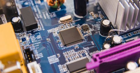
In this multi-board project article, we’re continuing where we left off creating an Arduino-style shield for an STMicroelectronics Nucleo-64 evaluation board. In this project, everything is getting far more integrated, taking us closer to a finished product. We’re going to integrate the microcontroller onto our board and add batteries, charging power management, and wireless networking. In the process, we’ll talk about surface mount sub-assemblies, and why you might want to separate part of your project schematic into its own board which can be used as a surface mount module.

As we discussed in the previous article, there are many reasons to separate your schematic into multiple boards. In that article, we mostly discussed risk reduction and optimization of board areas. Surface-mounted modules are probably not going to help you much with optimizing your product’s volume, and are unlikely to be as useful for prototyping purposes. Surface mount modules are typically going to be the same as other components - permanently fixed to your board unless you take on some serious rework.
EnviroSense Project
Our EnviroShield project is getting a big upgrade in this article - we’re taking it out of the prototyping phase where it was a Nucleo shield and building a standalone product. Ideally, this will be fully integrated into a mechanical housing featuring a passive radiation and moisture shield - but that’s beyond the scope of this article.
As with all my projects, this project is open source and free for you to use as you wish. You can find all the design files on GitHub. Of course, there is no warranty, guarantee, or liability associated with the project files as they are licensed under the MIT license.
As this is now going to be intended for indoor and outdoor uses, we also need a way to get our weather in PCB data back to a database, so we’ll be adding a Microchip ATWINC1500-MR210PB WiFi module.
In this project, we’re building the host board - but we’ll mostly be talking about how and why you would build your own surface mount module. The Microchip WiFi module is a perfect example of why you would create your own surface-mounted board.
Why Create a Surface Mount Module?
Certification
Intentional radiator certification is expensive. If you’re building custom wireless module designs into your products, it may make sense to move the radio hardware to its own sub-assembly you can separately certify. If you have multiple products using this custom radio wireless module design, you may be able to certify them under the much cheaper Unintentional Radiator class, as they integrate a pre-approved intentional radiator module.
You may also find this highly applicable to voltage regulators, motor drivers, or LED drivers that require certification such as for railway, automotive or medical applications. The Microchip ATWINC1500 module we’re using in this project is a perfect example of this approach. I could easily integrate the RF chip directly onto the board, however, certification costs would jump considerably.
Cost Reduction
If a small portion of your hardware requires a specialized PCB substrate, specialized PCB features like plugged or blind vias, or a higher layer count - you may find some savings by moving that portion of the project to its own sub-assembly. As the non-specialized area of your circuit board grows, you are paying a premium price for circuit board features you are not necessarily taking full advantage of.
Separating out the specialized portion of your project also makes the reuse of that schematic block much cheaper and easier in the future. You can simply place that existing wireless module design onto a non-specialized board and take full advantage of its features.
Standardization
If you find you are reusing schematics across multiple projects that have substantial engineering costs or risk laying out the board, it can be a good time to make a sub-assembly. A common example of this is a high-performance or high-reliability switched-mode voltage regulator. Isolated regulators are also commonly split into sub-assemblies.
Separating a portion of the design which has significant engineering investment, allows for rapid reuse without a major engineering cost to qualify the design integrated into a new circuit board.
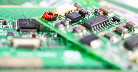
Module Surface Mounting Strategies
When creating your own surface mount module, you need to consider how your new module will attach to the host board. If you are going to be making large volumes of wireless module designs, you will likely need to evaluate both of the most common methods with your assembly process to determine the highest reliability and ease of assembly.
Land Grid Array
When selecting components you’ve almost certainly come across Land Grid Arrays (LGA) - bare pads under the IC or assembly. If you have a large number of connections to make in a small space, LGA can be an ideal approach. The major disadvantages are the same as any other LGA component - difficulty inspecting the joint and challenges with prototyping. You may also find additional costs with your board assembly partner due to the extra machine setup time - involving your board and assembly partners early in your design process can greatly improve your reliability and reduce your cost.

Source: U-Blox NORA-B106 on Digi-Key
You should avoid via in pad on both the host and module boards to ensure you don’t create air pockets in the solder, or thieve the solder through capillary action.
LGA is also highly cost-effective for module manufacturing. Some board manufacturers may charge more for castellated pads.
Castellated Pads
Many commercial modules utilize castellated pads for their modules, and with good reason. Castellated pads are highly reliable and very easy to hand solder and inspect. Due to solder wicking up the side of the board, you can also achieve good current density.
A castellated pad is effectively a plated through hole that is routed in half during the board manufacturing process. The routing toolpath in your panel will pass through the center of the hole, leaving a plated scallop on the board edge that has a pad on the top and bottom of the board.

Source: DIGI Xbee Pro XB8X on Digi-Key
Only having pads on the board edge also makes routing the host board easy, and will not interfere with via or track placement on the module board. The edge pads can be directly connected to a track or plane on any layer, which may make routing to the interconnect pads easier on the module.
Castellated Pad Design
It’s hard to go wrong with castellated pads, however, there are some things to consider which will set you up for success. If you’re new to creating castellated pads, it's worth downloading Altium files for commercial modules where they are available from the manufacturer, as I have done for the ATWINC1500 module I’m using in this multi-board design. Looking at the pad stack up and layout of commercially successful modules in a similar class to the module you are creating can give you some ideas on what works well before you begin your own experimentation.
Asymmetric Pad
When creating a castellated pad, the stack-up will almost always be asymmetric. The top and inner pads are typically going to be round and sized just as any through-hole pad or via would be. The bottom pad however is typically going to be enlarged to provide greater copper area and solder contact. This makes the castellated pad able to be used reliably with solder paste stenciled boards as well as hand soldering.
Edge Plating
If you require higher current density or even greater reliability you can also have the edges of the board plated beyond the through-the-hole. This plating is typically added to the width of the bottom pad, providing more contact area on the side of the module. Most board manufacturers will charge more for this service and low-cost high-mix board manufacturers may simply ignore this if they even notice the fab note.
A Good Starting Point
If you’re not short on edge space, start with larger pads for your initial prototypes. As you begin to feel more comfortable with the process and see the results of your initial modules you can begin to optimize the size downwards if necessary.
Microchip ATWINC1500 Pads
As an example of this, the Microchip pads on the ATWINC1500 module have a 0.635mm plated hole and a square 0.8mm pad for all layers. They have an additional 1.7 x 0.8mm round pad on the bottom layer (shown below moved to the left, to show they are separate).

Microchip recommends a 0.8 x 1.9mm pad on the host board, with the pad centered on the module outline.
My Castellated Pads
I’ve always done things a little differently to the Microchip example above, preferring to specify the full pad stack in a single pad.
My pads for RF modules typically have a 0.4mm plated hole, with a 0.8 x 1mm rectangular top pad. The bottom pad is 0.8 x 2mm centered on the hole, providing a 0.8 x 1mm exposed copper area under the board. The surface mount pad on the host board for these pads is 0.8mm wide, and 1.8mm long centered under the module outline.

For lower volume boards that are almost certainly going to be hand soldered, I’ll use larger holes where pin density isn’t critical. These have a 1.2mm plated hole, and a 1.5 x 2mm top pad with a 2.5 x 2mm bottom pad. These have less exposed copper under the board, as the larger plated hole on the side will provide most of the solder contact when hand soldering them to the host board.

Your Own Wireless Design Modules
When you create your own module, you should create your castellated pads as a single footprint/symbol, as this will make creating a multi-board project easier, and also ensure no single pad or cluster of pads can be accidentally moved causing alignment issues in the future.
Designing the Host Board
As mentioned earlier, we’re going to be taking our previous sensor and LCD display schematic and making it a standalone board. Initially, this board is going to be developed using a library part that has the WiFi module as the STEP model embedded in it. Many company libraries utilize this approach to multi-board design, however, it is less than optimal. With Altium’s impressive MCAD-ECAD integration, working directly with the board design makes more sense than exporting a STEP model of your module and re-importing it - especially early on in the design phase. As your module and host board requirements evolve, using a multi-board assembly allows you to ensure everything is kept in sync.
Once we have the board design completed using a library component, I’ll show you how easy it is to switch your existing library-based multi-board projects over to a footprint + multi-board assembly.
To make this hardware standalone and able to operate outside as a weather board design station we need a power source. I’m using the STM32L031K microcontroller which will be configured for very low power consumption, however, I want to ensure the board can continue to operate without external power for some time if required. I’m using two 18650 batteries just like I did in my 12V UPS project, however this time I’m using a different charger IC due to chip shortages and different requirements.
I would like my weather board design station to be solar powered, however, I’m located in the very far north of Scotland where in winter we have 5-hour-long days and can be trapped in a fog bank or dense cloud for days at a time - not exactly ideal conditions for solar powered devices. Using two 18650 batteries will allow me to run the weather station for around 6 weeks without external power if necessary. I also have a massive 6000uF capacitor on the input, to help deal with varying light conditions, keeping the charger running optimally.

I’m using the Microchip MCP73213 two-cell lithium battery charger IC for the project. It has a wide input voltage range which works well for either solar power or AC power if used indoors as well as programmable current. I’m specifically using the 8.2V charge model, despite my batteries being 8.4v maximum charge. As I expect these batteries to be at full charge most of the year, leaving them in a slightly less than the full state should improve their lifespan, and with such high capacity, the small hit to capacity shouldn’t be noticed. I have the charge current selectable through a slide switch, so it can be set to a low current for solar-powered applications, or fast charged by an AC adapter if needed.
Rather than using a battery monitoring IC, I’m taking the simple voltage cutoff route in the event the batteries are fully depleted. I’m using a linear regulator for this design, the Analog Devices ADP7105, which has an Under Voltage Lock Out pin to switch the regulator off if the battery voltage goes too low. Typically running a 3.3v device on a linear regulator from an 8.4v supply would be considered very inefficient, and not fantastic for battery life. After a lot of searching for high-efficiency light load-switched mode regulators that are in stock, I found the linear regulator to be far more efficient overall.
The challenge with this device for a switched mode regulator is the WiFi module, with a transmit current draw of 290mA, however, if we transmit data every 10 seconds then the remaining 98.5% of the time the current draw is likely to be in the low double-digit microamps where a switched mode regulator really struggles. In this case, taking the efficiency hit on the transmit current is well worth it for the relative efficiency and reliability at a low current.
Layout-wise, I have separate ground pours for each of the potential temperature zones, keeping the regulator and charger at the top of the board with the WiFi module. I also have slots in the board around these potential heat-generating components in an attempt to further break the thermal conductivity of the temperature sensor. Just as with the shield, the temperature sensor is at the bottom of the board in its own thermally isolated region.


Switching to a Multi-Board Assembly
Up till now, this project has used a library item for the RF module, which is how your company might currently be dealing with internal sub-assemblies. I downloaded the Altium files for the board from Microchip’s website. As the design files use a single footprint for the castellated pads all I needed to do was tell Altium Designer the connector is for a multi-board project by adding a parameter called “System” to the schematic symbol and giving it the value “Connector”. Preparing the sub-assembly board for multi-board connection is that simple.

For the host board, I had to do a little more work, as I already had a footprint with a STEP model in it. I copied the symbol and footprint files from my library into the project folder so I would have a local copy to modify.

In the footprint, I deleted the 3D body, then added the footprint to the schematic symbol. After changing the symbol in my schematic to the new local symbol, I added the System = Connector parameter to the symbol. Finally, I updated the PCB document from the schematic, and then on the PCB ran an Update From PCB Libraries to refresh the footprint.

The PCB now has a footprint with no body and is marked as a multi-board connector ready for assembly.
Creating the Multi-Board Project
To add our RF module board to the host board, we need to create a new multi-board project. Creating a new multi-board project is almost the same as a typical PCB project, except we choose Multi-board rather than PCB under the project creation screen.

Next, we add a multi-board schematic and two modules. Each module is given a title and a project/board is selected for the module.

To add the connectors we set up earlier, we go to Design -> Import Child Projects which will add the connectors to the modules.


Then we can add a direct connection between the two modules. Altium Designer wasn’t able to automatically match up the connections for the two modules this time, so we can click on one of the connections and in the properties window manually assign the mating pin.

With the pin mated correctly, we can add the multi-board PCB to the project, saving it as soon as it has been added. Then, from the schematic, go to Design -> Update Assembly to import the modules to the multi-board PCB. Depending on the complexity of your hardware, and the specs of this machine this might take some time. However, for this relatively simple project, it took under a second on my computer.

Rather than using the mating tools which we used in the previous article, I’d like to instead demonstrate that we can arbitrarily position the multi-board components anywhere we wish if that is what the design calls for. By clicking on the radio module, we can use the View Gizmo to drag it into place on our host board.

Outcome
In this article we have built an environmental sensor board that could act as a simple weather station for indoor or outdoor use, demonstrating the usefulness of a pre-certified RF module sub-assembly. We have discussed how and why you would create a sub-assembly module for your own projects. Using a multi-board assembly rather than a static 3D model in a library for custom surface mount modules ensures your boards stay in sync throughout the design process, and allows superior mechanical integration between the boards.
I also have a Davis Instruments Vantage Pro2 weather station, so it will be interesting to compare the long-term data from this weather station project to a NIST-calibrated product.
How will multi-board assemblies save you time, and increase your productivity? Talk to an expert at Altium now to find out.
About Author
Related Resources
Related Technical Documentation
Table of Contents
Design to Release, Without the Friction
- Keep reviews tied to the right version
- Reduce handoff confusion and rework
- Spot sourcing and release risk earlier
- Work solo, share when needed
Get Started
Thank you, you are now subscribed to updates.

