


Guide to PCB Terminology for Altium Designer


Understanding more about PCB design starts with learning the lingo.
ALTIUM DESIGNER
When working with a PCB design software tool, it’s best you know what it is you’re working with.
Whether you are just starting out in the PCB design industry, or you’ve been at it for a long time, you will more than likely run into terminology that you aren’t familiar with. There are technical terms in the electronic design industry that you may never have had exposure to. For instance, if you’ve never designed a flex circuit you may not know that the base material of these designs is a flexible polymer film. There are also descriptive words that have been around for so long that you may not know their origin. For instance, why is it that the main printed circuit board in microcomputers is called a “motherboard” instead of something else?
To help we have compiled a list of some of the more common words and terms used in the PCB design industry. This is not a complete list, but it should help to give you a start on what is what.
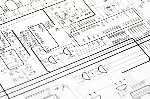
Schematic PCB Definitions
The PCB design industry is loaded with terminology, so much so that to one giant list may be a little overwhelming. To help we are going to break these lists down into general areas of PCB design. To start with, here are some general terms that are used throughout the industry:
ASCII:
American Standard Codes fкor Information Interchange.
Assembly House:
A factory that mounts components to PCBs.
Board:
A printed circuit board.
CAD:
Computer-Aided Design, CAD tools are used to design PCBs for manufacturing.
Circuit:
A group of electrical components which when connected together perform a specific function.
Components:
Devices or parts represented as symbols on the schematic whose physical footprints will be placed on a PCB layout.
DFA:
Design for Assembly; design specifications that target the PCB assembly process.
DFM:
Design for Manufacturability; to design a PCB so that it can be manufactured.
DFT:
Design for Testability; to design a PCB so that specific tests may be performed.
EDA:
Electronic Design Automation.
Electrical Connection:
When two or more parts of a circuit are connected together and conduct electrical signals.
Fabrication House:
A factory that builds the PCB.Flex Circuit:
A circuit board made from a flexible polymer film permitting it to bend in order to work around obstacles or plug into other circuit boards and devices.
High-Speed Design:
Designing a printed circuit board so that the high speed or high-frequency signals are transferred at peak functionality without signal degradation due to crosstalk and other interferences.
IC:
Integrated circuit; an electronic package that contains multiple components.
Manufacturing Process:
A general term that refers to both PCB fabrication and PCB assembly.
MCM:
Multi-Chip Module; a package that contains two or more IC’s connected together.
Multi-layer PCB:
A PCB that is made up of more than two (top and bottom) layers.
PCA:
A Printed Circuit Assembly
PCB:
A Printed Circuit Board
PCB Assembly:
The process of soldering and attaching components to a fabricated PCB to make it into a PCA.
Printed Circuit Board:
A mechanical structure made from layers of core dielectric materials and layers of metal connections to support and connect electrical components to complete circuits.
PCB Design:
The process of laying out a printed circuit board from a schematic.
PCB Fabrication:
The process of creating a PCB from base materials.
PCB Layout:
The process of placing components and routing traces to create a printed circuit board.
Printed Wiring Board:
The same as a Printed Circuit Board.
Printed Wiring Assembly:
The same as a Printed Circuit Assembly.
SMD:
Surface Mount Device.
SMT:
Surface Mount Technology.
Solder:
A low-melting alloy used for joining metals such as component leads to metal pads on a PCB.
Substrate:
A substance or layer that underlies something. In a PCB it is made of laminate materials as specified in IPC-2221.
Surface Mount Technology:
Components whose leads are soldered onto surface pads representing its footprint on the PCB.
Through-hole Technology:
Components whose leads are inserted and soldered into drilled holes representing its footprint on the PCB.
Wiring Board:
A circuit board that is mounted with pins that are physically wired together in a process called “wire-wrapping”.
To start the design, a circuit designer creates the design and draws the circuit in a schematic capture tool, representing components and their connections. Using the schematic, a PCB layout designer uses the schematic to import components and net connections into a PCB layout tool. Once imported the component footprints and nets are used to design the PCB layout. Here are some definitions that are associated with the schematic capture process:
Active components:
Components on a PCB that are capable of controlling current flow by means of an external electrical signal, such as transistors
ASIC:
Application-specific integrated circuit.
Capacitor:
A passive electronic component that consists of two conductive plates separated by an insulating dielectric. The plates will store voltage until discharged.
Capacitance:
The amount of charge that can be stored at a given voltage.
CMOS:
Complementary metal-oxide semiconductor. This is a common transistor Architecture.
Current:
The amount of charge that flows past a given point or through a device.
FPGA:
Field Programmable Gate Array.
Impedance:
The measurement of the opposition to electrical flow in AC systems in units of ohms. Consists of resistance and reactance.
LED:
Light Emitting Diode.
Nets:
The connections on a schematic that create the connectivity between
component pins.
Passive Components:
Circuit board parts that do not actively produce or control signals such as IC’s, but instead have a passive effect on the circuit. Resistors and Capacitors are examples of passive components.
Resistance:
A measure of the opposition to electrical flow in DC systems measured in Ohms.
Resistor:
A component that is designed to resist a portion of the amount of electrical current that passes through it.
Semiconductor:
An electronic device such as a transistor, diode, or IC manufactured from semiconductor materials.
SPICE:
Simulation Program with Integrated Circuit Emphasis; a simulator for analyzing signals in a schematic.
Transistor:
A basic active solid-state control device that allows or disallows current flow between two terminals, based on the voltage or current delivered to a third terminal.
TTL:
Transistor-to-transistor logic.
Volt:
Unit of measure for the electrical potential between two points. An electrical potential of 1 volt will push 1 ampere of current through a 1-ohm resistive load.
Putting Schematic Definitions to Work
Now that we’ve seen some of the terminology associated with PCB design and schematic capture, let’s look at some specifics of creating a schematic.
- Here are some tips to organize your schematic to best serve the needs of high-speed design.
Learn More about the different considerations of creating a schematic.
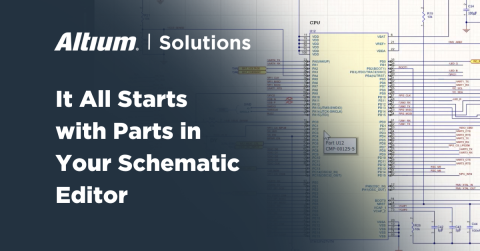
- Here are some details on how to work with components and other functionality in Altium Designer’s schematic editor.
Learn More about how to use the schematic capture editor in Altium Designer.
- Here is a brief tutorial, on how to transfer schematic information to your PCB layout within Altium Designer.
Learn More about creating an Altium Designer layout from your schematic.

Creating the schematic of a PCB design
Layout PCB Design Glossary
Once your schematic is complete, you are ready to begin the physical layout of your PCB design. To start with you will want to learn more about the parts, processes, and materials that you will be working with:
Annular Ring:
The plated ring of metal around a drilled hole in a PCB. The outer diameter is the size of the metal pad while the inner diameter is the finished (plated) hole size.
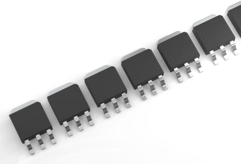
BGA:
Ball grid array; a component package.
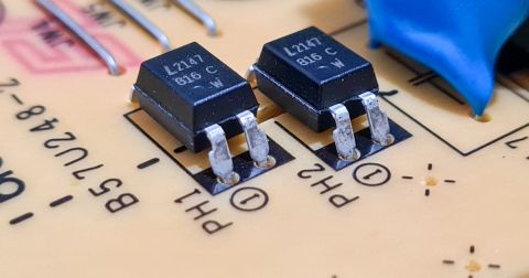
Component Leads:
The metal pins of an electrical component that connect the interior of the device to the solder pads of a PCB.
Component Placement:
The process where the PCB designer arranges component models on a PCB design in a CAD system.
Conductive Material:
Metal, such as copper, that is used for traces, vias, and pads on a PCB to conduct electrical signals.
Conductors:
Traces or solid areas of metal on a PCB that conduct electrical signals.
Copper:
A metal used in the fabrication of PCBs for its low resistance to the conduction of electrical signals.
Cross-sectional Area:
A 2D space; used to view the interior layers and construction of a PCB.
Dielectric:
An insulating material, used in PCBs to limit electrical interference between adjacent layers. Also used between plates of capacitors to prevent current flow through the device.
DIP:
Dual In-line Package, a component package.
DRC:
Design Rule Check; performed to make sure that the design has no clearance, dimension or other violations that may prevent its manufacture.
Dual In-line Package:
An electrical component with two rows of pins.
FCC:
Federal Communications Commission; an organization that sets rules and regulations for PCBs that contain devices that radiate energy.
Heat Sink:
A mechanical device connected to a heat-producing component in order to conduct heat away from it.
Hole:
In a circuit board the hole will be either drilled or milled (routed) and can be plated with metal or not plated. May be used for conduction, as with vias, or for mounting.
Insulating Material:
See dielectric.
Layer:
The different metal layers of a PCB. These can be signal layers (traces) or plane layers. Although each metal layer has dielectric and/or prepreg layers between them, normally only the metal layers are referred to as a “layer” in a PCB.
Pads:
Small areas of metal on a PCB that the leads or pins of components will be soldered onto or into depending on whether the components are surface mount parts or thru-hole parts.
PLCC:
Plastic Leaded Chip Carrier; a component package.
QFP:
Quad flat pack, a very common component package.
Reference Designators:
Unique identifiers or labels on a PCB that identify each component.
Slot Hole:
A hole in the PCB that is rectangular instead of a round drilled hole.
SOIC:
Small outline integrated circuit, a component package.
SOP:
Small outline package, a component package.
SOT:
Small outline transistor, a component package.
Solder Mask:
A layer applied to a PCB to mask solder from certain areas. Primarily used to protect the board surface and prevent solder bridges. Most of the PCB will be masked except for the metal pads that need to be soldered.
Solder Paste:
Solder in a paste form that is applied to the metal surface mount pins for
the reflow solder process.
Stackup:
The design of the PCB’s layers; including material type, dimensions, etc.
TSOP:
Thin small-outline package, a component package.
TSSOP:
Thin shrink small-outline package, a component package.
ZIF:
Zero Insertion Force; IC sockets that clamp the IC pins using a small lever after insertion sparing the component from being worn out.
After the components have been placed on the printed circuit board during layout, it is time to route the traces of the design. Here are some definitions that cover different aspects of trace routing a PCB:
Backdrilling:
Also known as control depth drilling, this is used to remove the unused barrel of a thru-hole in order to remove unwanted stubs on high-speed signals.
Crosstalk:
A phenomenon where a signal on a trace is capacitively coupled to an adjacent trace.
Daisy Chain:
A method of trace routing to connect devices in series.
DDR Routing:
The methodologies and topologies of trace routing Double-Data-Rate memory circuits.
Differential Pair Routing:
A method of routing a pair of balanced traces to carry differential (equal and opposite) signals across a PCB.
Guides:
When the schematic information is first transferred to the PCB, the nets are represented by “guides”. These guides are then turned into metal traces during the trace routing portion of PCB design.
Matched Length Routing:
Routing traces such as the two traces of a differential pair so as to match their total length within specific tolerances.
Trace:
The metal connections between pads and vias on a PCB that carry the electrical signals.
Trace Routing:
The process where the PCB designer creates the traces on a PCB.
Trace tuning:
Introducing a serpentine pattern into a trace in order to match its length to another.
Via:
Small hole drilled in a PCB and plated that allows a trace to connect to another trace on a different layer of the board that are part of the same signal path.
Understanding More about PCB Layout
The following resources will help you to be better prepared for your PCB layout.
- In this brief tutorial, you will see how to create power and ground planes using Altium Designer.
Learn More about how to create power and ground planes in Altium Designer.
- See how Altium Designer gives you great control over the trace routing line widths and spacing.
- Altium Designer gives you many different options when doing your trace routing, here is an introduction to some of them.
Learn More about routing techniques that you can use in Altium Designer.

A PCB design system with multiple tools that are easy to work with is a huge benefit
Altium Designer; Raising the Bar on a New Glossary
Once your PCB design is complete, it is time to get it manufactured. Here are some of the definitions for terms that you will encounter while working within the PCB fabrication and assembly processes:
Ambient Temperature:
Temperature of the air surrounding a component.
Base Material:
The core material of a circuit board, such as FR4.
B-stage Resin:
A single element epoxy system instead of combining elements to create epoxy.
BOM:
Bill of Materials; a list of all parts on a PCA. The BOM will contain the
reference designators, part numbers, and quantities of each part in
addition to other information needed to build the board.
Drill File:
An ASCII file containing X & Y coordinates for drilling holes in a circuit
Board.
Drilled Hole:
A hole in a circuit board that can either be plated through with metal or not
Plated.
Epoxy Resin:
Used to coat and encapsulate PCBs.
Excellon File:
ASCII files used with CNC drilling, milling, and routing machines.
FR4:
A base material used for the substrate of PCBs composed of woven fiberglass cloth with an epoxy resin binder that is flame resistant.
Functional Test:
A method of testing an assembled board to assure that circuitry functions within specifications. The board is tested using a combination of connectors and pin probes.
Gerber Files:
ASCII files containing PCB design information, including X & Y coordinates for the pads, vias, traces, and other elements needed to create a circuit board.
Hazardous Substances:
The byproducts of chemicals and materials used in the fabrication of PCBs that are hazardous.
In-circuit Test:
A method of testing an assembled circuit board for manufacturing defects. The board is tested on a bed of probes to test for shorts, opens, resistance, capacitance, and other basic functions.
JTAG:
Joint Test Action Group; an industry standard for testing PCBs after manufacturing.
Keep-Out Areas:
An area of a PCB where trace routing, vias, components, or other mechanical fixtures are not allowed. These can be managed with keep-out zones in the CAD system.
Laminate:
Laminate is the result of lamination, which is the process of combining the core materials of the PCB, such as FR4, with the copper layers and prepreg through heat and pressure.
Molten Solder:
Solder that is melted and ready to have a PCB run through it in order to solder the leads of the components.
Panel:
A standard size and shape board that contains multiple PCBs for manufacturing attached within it. This allows the smaller PCBs to be manufactured in greater number, and more efficiently.
Plating:
The electrochemical process of coating the metal pads and the inside of drilled holes with metal on a PCB.
Prepreg:
Layers in a PCB buildup that are composed of uncured FR4 to glue together core material and copper foil, and ready to be hardened with heat and pressure in the fabrication process.
Purchase Order:
A method of ordering materials and parts.
Reflow Solder:
The process where solder paste applied to surface mount component leads is passed through an oven to melt and reflow it in order to make a good solder joint.
Solder Joint:
Where the solder is melted to combine the metal component lead to the metal pad on the PCB.
Spring-loaded Pins:
Pins with springs in them. These are often used for in-circuit testbeds so that the pin will constantly make a good connection to the metal that it needs to test.
VIPPO:
Via-in-pad plated over. A via structure that is plated over with copper so that solder does not wick into the via.
Wave Solder:
A bath of molten solder that a PCB is run over in order to solder the leads of through-hole devices.
Don’t Settle for Anything Less than the Best; Altium Designer
There’s a lot to understanding the world of PCB design, and these definitions are just a start. Take a look at how using Altium Designer can help you with all aspects of your design.
- Altium Designer’s schematic capture editor is easy for the first time user while powerful enough for the most complex designs.
See how Altium Designer’s schematic capture is intuitive and easy to learn.
- Working between the schematic and the layout in Altium Designer is made simple thanks to the unified design environment.
- With smaller budgets and less design time, use Altium Designer’s native 3D engine to check and work with your component placement before you go to manufacturing.
- Altium Designer gives you many different options for routing that will make your job easier as a PCB designer.
See how Altium Designer’s intelligent interactive routing will make you more productive.
Designing a printed circuit board is not a small undertaking. You need to understand all aspects of what you are doing, and you can’t afford to use anything less than the best PCB design software available; Altium Designer.

About Author
Related Resources
Related Technical Documentation
Table of Contents
Design to Release, Without the Friction
- Keep reviews tied to the right version
- Reduce handoff confusion and rework
- Spot sourcing and release risk earlier
- Work solo, share when needed
Get Started
Thank you, you are now subscribed to updates.


