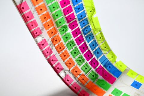


Flex PCBs: Flexible Circuit Signal Integrity for Mesh Ground Planes

At a Glance
Even flex PCBs need a ground plane. Mesh ground planes can provide a 0 V reference in your PCB, but they have particular signal integrity requirements.


Ultra-high speeds on flex and rigid-flex boards are inevitable as these boards are finding greater use in advanced electronics. These systems also need ground layers for isolation, and for separating RF and digital references for wireless protocols. With high speeds and high frequencies comes the potential for signal integrity problems, many of which relate to the placement and geometry of the ground plane in a PCB.
A common method for providing a consistent 0 V reference in flex and rigid-flex boards is to use a hatched or meshed ground plane on the flex ribbon. This provides a large conductor that can still provide shielding over a broad frequency range while still allowing the flex ribbon to bend and fold without excess rigidity. However, signal integrity problems arise in two areas:
- Ensuring consistent trace impedance,
- Shielding and isolation, and
- Preventing fiber weave-like effects in the hatching structure.
In this article, we’ll look deeper at the signal integrity problems that come from hatched ground planes and what you can do about them.
Mesh Ground Plane Design
In the most basic sense, hatching works just like any other ground plane. It’s meant to provide a consistent reference so that a trace can be designed to have the desired impedance. Any of the common transmission line geometries (microstrip, stripline, or waveguides) can be placed in rigid-flex or flex PCBs with a meshed ground plane. Placing a hatched copper region on the surface layer of the flex ribbon provide nearly the same effects as solid copper at low frequencies.
The common configuration for stripline and microstrip routing on a flex ribbon with mesh ground planes is shown below.

This mesh structure can be used in rigid boards, but I’ve never seen this in practice nor have I had a client request it. Instead, the mesh pattern is used in flex/rigid-flex boards to balance the need for impedance control with the need for a reasonably flexible ribbon. Whether you’re designing the traces or the hatch pattern, follow best practices for static and dynamic flex ribbons and the IPC 2223 standards.
Impedance Control
One option for working with single-ended or differential pairs is to place solid copper in the plane layer directly below the traces and place a mesh structure elsewhere in the circuit. If the routing becomes very dense, then you’ll need to use mesh everywhere. If you opt to use mesh, you’ll have greater flexibility, but lower shielding isolation and modified conditions for impedance control.
As shown above, the mesh plane structure has two geometric parameters: L and W. These two can be combined into a fill factor, or the fraction of the mesh area covered with copper. Changing these parameters has the following effects:
- Opening the mesh area (increasing mesh opening by increasing L) increases impedance assuming other parameters are held constant. It also makes the ribbon easier to bend (less force).
- Increasing W while holding other parameters constant closes the mesh area, which increases impedance. It also makes the ribbon mode difficult to bend (more force).

The other parameters that govern impedance for standard geometries have the same effects when working with a mesh ground plane. Once you get to high frequencies, you’ll excite non-TEM modes around your transmission lines, and you may even see some fiber weave-like effects.
Fiber Weave Effects in my Flex Ribbon?
This is where a mesh ground plane in a PCB gets very interesting as the mesh pattern can start to resemble the glass weave pattern used in FR4 and other laminates. As a result, we’re now back in a situation where we have to worry about fiber weave effects in a normally smooth, relatively homogeneous substrate material. These effects occur when the bandwidth of a travelling signal overlaps with one or more resonances in the mesh structure. For L = 60 mil on polyimide, the lowest order resonance would be 50 GHz.
An early study (see this article from Hindawi) showed that these hatched structures, whether on a rigid or flex PCB substrate, can produce strong emission when a digital signal propagating on a track across the mesh ground plane. As more flex applications open up at higher frequencies, I would expect these effects to be worse in a flex ribbon with a mesh ground plane for a few reasons.
Higher-Q Resonances
Just like in a regular glass weave substrate, the mesh forms a cavity structure that can support resonances when excited at specific frequencies. These resonant cavities in a mesh ground plane will have very high Q-values as the walls of the cavity are highly conductive (copper). Therefore, there will be lower losses and higher-Q resonances. This leads to increased cavity emissions and resonant power loss.
Open Mesh Has Low Isolation
A solid ground plane would normally ensure any radiated EMI from fiber weave cavities was emitted along the edge of the board. Because a mesh ground plane has open cavities, it provides less isolation and can also radiate along the surface of the flex ribbon. This has a reciprocal effect: when a trace can more easily emit radiation, it can also more easily receive external EMI.
To solve these problems, use tighter meshes, just like you would use a tighter glass weave to prevent fiber weave effects. Flex and rigid-flex PCBs will continue to be a part of the PCB landscape and are becoming more advanced with newer manufacturing capabilities. Tara Dunn’s announcement of 1 mil trace width fabrication capabilities can be a real game changer for high speed, high density flex PCBs by allowing fabrication of smaller mesh ground plane patterns.
Mesh Ground Plane Example
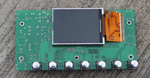
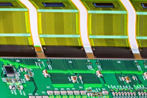
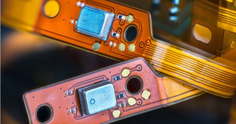
An example of a well-constructed mesh ground plane can be found in the open-source laptop project being spearheaded by Lukas Henkel. The image below shows an example with a mesh ground plane being applied on a 1 mil thick flex ribbon for a webcam. This flex PCB is intended to support MIPI CSI-2 routing from an edge FPC connector to a webcam that is soldered directly onto the flex ribbon. The geometric parameters are as follows:
- Copper trace width: 0.1 mm
- Opening size (repeating element): 0.283 mm
In this example, multiple hatching regions are used to define ground in different portions of the flex ribbon. There is also a large solid region in the hatch plane, which is being used to separate the high-speed CSI-2 signals from lower speed configuration signals and GPIOs in the top portion of the hatching region. Once you're ready to route signals above the hatching region, the routing tools will work exactly the same as routing over a solid plane or solid polygon.

This kind of hatching does not need to be drawn out manually by routing traces. Instead, Altium Designer includes a feature that will apply the hatching automatically on a polygon, and the selected hatching will appear once the polygon is repoured in the PCB Editor. This feature can be applied on rectangular polygons, curved polygons as shown above, or on irregular polygon pour.
Simulating Routing Over Mesh Ground
Mesh ground planes can technically be simulated just like any other structure in a PCB, but the challenge comes from more computational power requirements due to the more complex structure of the mesh ground. The openings in these mesh layers creates a more complex simulation mesh that is then used to solve Maxwell's equations, which then requires longer computational time. For example, an S-parameter simulation for a single differential pair over a mesh plane can require over 1 hour of simulation time (based on simulations of the PCB cross section), while the same differential pair and stackup with a solid copper ground plane would take under 1 minute when analyzed with the same numerical method.
The above facts make the determination of impedance for routing over mesh ground very difficult. Another problem that arises is the lack of clear data from manufacturers. Not all manufacturers keep data on impedance over mesh ground planes, primarily because the impedance depends so heavily on the fill factor and orientation of the copper mesh. Because the parameter space is so large, flex PCB manufacturers that do keep these data probably only have valid test data for a few parameterizations and for specific polyimide products. Therefore, if you need high-speed routing on flex for an advanced product, consider investing in a 3D field solver simulation tool.
No matter how you plan to design your flex or rigid-flex PCB, Altium Designer® has the tools you need to properly design a mesh ground plane for high speed designs. Altium Designer on Altium 365® delivers an unprecedented amount of integration to the electronics industry until now relegated to the world of software development, allowing designers to work from home and reach unprecedented levels of efficiency.
We have only scratched the surface of what is possible to do with Altium Designer on Altium 365. You can check the product page for a more in-depth feature description or one of the On-Demand Webinars.

About Author
Related Resources
Related Technical Documentation
Table of Contents
Design to Release, Without the Friction
- Keep reviews tied to the right version
- Reduce handoff confusion and rework
- Spot sourcing and release risk earlier
- Work solo, share when needed
Get Started
Thank you, you are now subscribed to updates.