


The Best High Voltage PCB Design Software Package


Of all the different boards a designer can create, a high voltage PCB design can be complicated and requires strict attention to safety. If not laid out correctly these boards can be safety hazards or can fail to function on first power up, leaving a designer with wasted time and effort. In the best case, the board will function reliably for a long period of time thanks to correct layout practices.
When you’re planning your next high voltage PCB design, make sure you use the best design tools for the job. Any circuit board layout program will let you arrange components and route traces around a board, but only Altium Designer checks your PCB layout against high voltage PCB design rules as it’s being created. We’ve compiled everything you need to know about successful high voltage PCB design so that you can be safe and successful.
ALTIUM DESIGNER
The only high voltage PCB design package built on a unified rules-driven design engine.
High voltage PCB design can be as complex as any high-speed digital design. Boards for high voltage systems can be space constrained and they carry important safety requirements. They also need to be highly reliable to ensure they will have a long life when run at high voltage and current. With so many design demands on high voltage PCBs, layout engineers need a complete set of design tools to help them satisfy all design constraints.
Considerations in High Voltage PCB Designs
High voltage circuit boards are normally used in power systems, such as in power generation, conversion, or distribution. These tasks may involve a range of voltages, and the PCB for this equipment must accommodate a range of power levels simultaneously. Here are a few of the points that need to be determined before starting any high voltage PCB layout:
- Maximum voltage level: The maximum voltage level in the board will determine the relevant safety standards that need to be obeyed and the distance between conductors in the PCB layout.
- AC vs. DC power: DC power systems are more dangerous than high voltage AC systems. However, high-power AC systems may still need isolation to protect the user from dangerous currents.
- Power topology: The topology of a power system also determines safety, as well as the components that are used to build circuits for the system. Different topologies will have their own design and layout rules to ensure stable power and prevent noise from reaching downstream circuits.
- Operating temperature: The operating temperature will be a major determinant of reliability and will depend on the power dissipated in conductors and components in the system. For resistive components and the PDN in your PCB, some power drop is unavoidable and will lead to a temperature increase in the system.
The electronics industry has addressed these aspects of high voltage design and many more by creating industry standards. These standards are intended to ensure the reliability and safety of high voltage power products.
Industry Standards on High Voltage PCB Design
Some of the important industry standards on high voltage circuit boards are the IPC 2221, IPC 2152, and IEC 60950-1 (now merged with IEC 60065-1 into the new IEC 62368-1 standard). When you have the best set of PCB design tools, the requirements in these important design standards can be encoded in your PCB project as design rules. This helps you design to the level of reliability and safety required in high voltage PCB designs.
- The IPC 2221 standard and IEC/UL standards state the required spacing between different conductors in a high-speed PCB as a function of the potential difference between them. An IPC 2221 calculator can help you automatically satisfy this standard.
- Two particular elements that need to be spaced properly in a high voltage PCB are traces and pads. Keeping these elements carefully separated prevents ESD at high voltage.
Learn more about setting trace and pad clearance rules to prevent shorts.
- Advanced high voltage circuit boards can be designed on a range of possible materials. Some unique materials include metal-core PCBs and ceramics.
Learn more about substrate material options for high voltage PCB design.

The spacing between these conductors should be carefully checked to prevent ESD during operation.
High Voltage vs. High Current PCB Design
High voltage PCB designs are often high current PCB designs except in some odd cases. For example, equipment like power supplies and high-power regulators need to receive a high voltage and may convert it to moderate voltage at high current. As such, some sections of the PCB may need to be designed to withstand the heat generated by high current.
There are two important tasks in high current design that help ensure reliability:
- Trace width sizing: Traces in a high current PCB need to be made wide enough to prevent high temperature rise. These requirements and a useful nomograph are specified in the IPC 2152 standards.
- Heat dissipation: When heat is generated in a high current PCB, the heat needs to be moved away from components to prevent them from exceeding their temperature rating. The heat generated in these boards can be removed with plane layers, fans, heat sinks, or by using a high thermal conductivity substrate with a metal housing.
When high current PCB design rules are used with the clearances defined for high voltage PCB designs, a designer can rest assured their board will be safe and will provide high current without excessive temperature rise.
Managing Heat in Your High Voltage PCB Design
Fans, heat sinks, exotic materials, and even liquid cooling can all be used to remove heat from a high voltage/high current PCB. However, a designer needs to determine the maximum temperature rise they can tolerate in the board to ensure reliability. Once this is determined, the trace width and other required heat dissipation measures can be determined. Once high voltage and high current design rules for your circuit board are determined, the best design software will check your PCB layout against these rules automatically.
- Once you’ve determined the allowed temperature rise in your PCB, you can use the IPC 2152 guidelines to determine the minimum trace width you need.
Learn more about determining the minimum trace width in a high-current circuit board.
- Just like other modern PCBs, high current traces may need to be routed through a via and onto an interior layer.
Learn more about the current carrying capacity of vias in a high current design.
- Using a PDN analyzer simulation tool can help you spot areas in the PCB where a current is excessively high.
Learn more about setting up and running PDN simulations in Altium Designer.

PDN simulations can help you identify areas where current is too high.
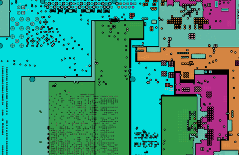
Checking High Voltage PCB Design Rules in Your PCB Layout
High voltage PCB design rules aren’t there to constrain your creativity, they are there to ensure your board is safe and will function when it is first started up. As you create your high voltage PCB layout, it needs to be checked against standard design tools to ensure safety and functionality.
In Altium Designer, you can encode all the important high voltage design requirements you need as rules and constraints. The layout features in Altium Designer are built on top of an online DRC engine, which checks your layout against design rules as you create it. This helps you catch and prevent errors early in the design process, and it helps prevent the extent of any redesigns that might be required for safety.
Create PCBs for Any Application in Altium Designer
The complete set of PCB design features in Altium Designer let you do more than just create high voltage circuit boards. You can design high-speed digital systems, high-frequency analog systems, mixed-signal layouts, and much more with a complete set of rules-driven PCB design and layout tools. No other circuit board design platform gives you this many easy-to-use design features.
- The DRC engine in Altium Designer is your key to successful high voltage PCB design. All the design tools in Altium Designer are built to ensure your board will operate as designed and will be manufacturable at scale.
Learn more about the PCB design environment in Altium Designer.
- When working on high voltage and high current designs, the PDN Analyzer extension for Altium Designer is ideal for examining current distribution in your PDN and identifying hot spots that could lead to failure in your circuit board.
Learn more about the PDN Analyzer extension for Altium Designer.
- Once your high voltage PCB design is complete and has passed all rule checks, you can share your data with your design team using the Altium 365 platform.
Learn more about PCB design collaboration in the cloud with Altium 365.

You can easily spot power integrity problems in your high voltage PCB design with the PDN Analyzer extension in Altium Designer.
The complete set of design tools in Altium Designer helps you gain peace of mind when working on your next high voltage PCB design. You’ll have a complete set of tools to help ensure your high voltage board operates as you intend and will be safe once it’s put into operation.
Altium Designer on Altium 365 delivers unprecedented integration to the electronics industry until now relegated to the world of software development, allowing designers to work from home and reach unprecedented levels of efficiency.
We have only scratched the surface of what is possible to do with Altium Designer on Altium 365. You can check the product page for a more in-depth feature description or one of the On-Demand Webinars.
When it comes to designing high voltage PCBs, it's important to ensure your layout is able to control and optimize electric field strengths for optimal operation and longevity. While the manufacturing process of high voltage PCBs remains similar to that of normal PCBs, careful attention to the materials you use, as well as their properties, are crucial to success. A thorough understanding of spacing rules, clearances, operating frequencies, and tried-and-true design techniques will go a long way in avoiding setbacks and potential challenges.

About Author
Related Resources
Related Technical Documentation
Table of Contents
Design to Release, Without the Friction
- Keep reviews tied to the right version
- Reduce handoff confusion and rework
- Spot sourcing and release risk earlier
- Work solo, share when needed
Get Started
Thank you, you are now subscribed to updates.


