Powerful Design Software that Leaves Nothing to Chance on Your PCB Fabrication Drawing

Whenever a design needs to be prepared for manufacturing, designers need to prepare multiple pieces of documentation to help them get into fabrication. In addition to supplying copies of design files, PCB designers need to provide standard fabrication and assembly drawings to thoroughly communicate their design intent to a manufacturer.
A PCB designer shouldn’t have to use external drafting tools to create a PCB fabrication drawing and other important design documentation. Instead, Altium Designer is the only PCB design software application that generates PCB fabrication drawings without the need for external CAD software. When you need to prepare a design for fabrication and assembly, here's how Altium Designer can help you stay productive.
ALTIUM DESIGNER
The best PCB design software with manufacturing planning features for professional PCB designers.
Schematic capture, simulation, synchronization, component placement, routing, and design rule checks. These are all familiar portions of printed circuit board design that designers have perfected over the years. However, there’s one final step needed to complete the job; the manufacturing deliverables. If those files aren’t created perfectly, all of your previous work may have been wasted. Your final printed circuit board will only be as good as your PCB fabrication drawing and other manufacturing files, and you can’t afford to send out anything less than the best.
Fortunately, the powerful PCB design software in Altium Designer is loaded with advanced tools to help you easily create schematics and your PCB layout. When you’re ready to start the PCB fabrication process, Altium Designer has many automated output features to help you panelize your designs, generate fabrication files, create assembly drawings, and source components for your design.
And of course, creating manufacturing drawings in Altium Designer’s Draftsman is as easy as setting up drawing templates and letting the tool do most of the work for you. A complete set of output job files will help ensure you always send out a complete build package to your PCB manufacturer. So relax and let Altium Designer do the job it was designed to do; help you create the best PCB designs possible.
How Your PCB Manufacturer Uses Your Fabrication Files
Your PCB manufacturer will use your fabrication files to build a bare board stackup that will eventually be used for assembly. The fabrication process follows multiple steps:
- Masking and etching copper-clad laminates for each layer in the PCB stackup
- Heating and pressing each layer into the completed PCB layer stack
- Drilling and milling mounting holes, through-holes, tooling holes, and slots
- Plating through-holes in an electrolytic plating solution
- Coating with solder mask and printing silkscreen
- Final cleaning and residue removal
Fabrication files are used to create stencils and choose tooling to fabricate the PCB, and to create CNC instructions for automated drilling and pick-and-place equipment. Fabrication drawings are critical for ensuring accurate stackup fabrication, but they can be time-consuming to create without the right PCB design software.
Prepare the PCB Fabrication Drawings Your Manufacturer Needs
To ensure accurate printed circuit board stackup fabrication, you need to give them high-quality drawings and output files. Your PCB fabrication drawing needs to include drill hits, dimensions, a layer stack diagram, and clear markings for different types of holes on each layer. Make sure to include this important information in your PCB fabrication drawings when preparing a design for manufacturing.
- A PCB fabrication drawing shows how a layer sack goes together and where drill hits are placed, and your manufacturer will use this as a guide to help them build the layer stack for your printed circuit board.
- Before the PCB stackup can be created, each layer is processed and etched using photoplotter data from Gerber files or another vector fabrication file.
Learn more about Gerber file formats and how to create them.
- Other fabrication files are needed to ensure a circuit board can proceed through the remainder of the fabrication process.
Learn more about what you need in a complete PCB manufacturing package.

Generate high-quality Gerber files and other deliverables in a single application.
What’s in a Complete PCB Fabrication Package
More than one fabrication run has failed due to incorrect or incomplete data being sent to a manufacturer. Every design that will be put into production needs to have a fabrication package with the following files:
- Gerber files in standard formats (RS-274-X or X2)
- A bill of materials with complete sourcing information and alternative components
- Fabrication and assembly drawings showing the PCB stackup information and component locations
- Netlists for automated testing and layout verification
- PCB testing data and testpoint descriptions
- Pick-and-place data for automated assembly
- NC drill files for placing vias and mounting holes in the PCB stackup
Altium Designer was created to allow users to complete design and manufacturing planning tasks in a single program. While other design software continues to place important design and manufacturing features into separate programs, Altium Designer keeps you productive by placing everything you need into a single application.
Generate Every PCB Manufacturing File in Altium Designer
PCB manufacturing requires a complete set of documentation, and Altium Designer gives you everything needed to generate your PCB manufacturing package. No external programs are needed and designs can be quickly converted into standard manufacturing deliverables in a single program.
- PCB designers should take time to learn about the fabrication process and how their designs are placed into manufacturing.
- There’s no need to worry about moving your data within the different tools in Altium Designer thanks to Altium’s signature unified design environment.
Learn more about the unified design environment in Altium Designer.
- Not all PCB manufacturers use Gerber files. Make sure you understand the differences between different types of PCB fabrication files before you begin your next manufacturing run.
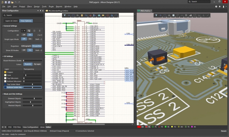
Altium Designer’s powerful interface helps you quickly generate fabrication and assembly outputs from your design data.
Powerful PCB Design and Manufacturing Tools in a Single Program
Before you can export your PCB layout into standard file formats for manufacturing and assembly, you need a complete set of features to create your design. Altium Designer has your needs covered with its complete set of PCB design and layout features, and all in a single program. Designs start with a professional schematic editor, where it’s easy to find and place components, and to run simulations of the design to ensure electrical functions are implemented correctly.
Next, Altium Designer lets you import your schematics as an initial PCB layout and start arranging components in your design. With a native 3D design and layout engine, and some of the most intelligent interactive routing tools available, Altium Designer can handle your toughest design challenges. The glue that brings this all together is Altium’s signature unified design environment that combines all these features and many more into a single application with an intuitive user interface.
Stay Productive with Automated Manufacturing Features in Altium Designer
The greatest part of Altium Designer is automation that helps a design team quickly create high-quality documentation without any external software. Manufacturing documentation generation is quick and easy with Altium Designer, helping you stay productive and ensuring accurate fabrication.
- Only Altium Designer brings a complete set of design and fabrication features into a single application. If you want to stay organized and productive, use the only fully integrated design application in the industry: use Altium Designer.
Learn more about the unified PCB design features in Altium Designer.
- The Draftsman package in Altium Designer makes it easy to create PCB manufacturing drawings.
- Altium Designer links you to your manufacturer through the Altium 365 platform, the only cloud service that is specialized for storing, sharing, accessing, and updating your PCB project data from anywhere.

Altium Designer’s Draftsman will help you to easily create a superior PCB fabrication drawing.
Altium Designer helps you get through fabrication and PCB assembly with a complete set of design and documentation features in a single application. No other PCB design software platform offers this many features in a single program, and only Altium Designer helps you operate with maximum productivity in a single application.
Altium Designer on Altium 365 delivers an unprecedented amount of integration to the electronics industry until now relegated to the world of software development, allowing designers to work from home and reach unprecedented levels of efficiency.
We have only scratched the surface of what is possible to do with Altium Designer on Altium 365. You can check the product page for a more in-depth feature description or one of the On-Demand Webinars.


