How the Fiber Weave Effect Influences High Frequency Signal Integrity

With many devices running at high data rates and incorporating RF functions, designs on some rigid substrates may need to accommodate an inconvenient phenomenon: the fiber weave effect. There are actually multiple signal integrity problems that can arise due to the fiber weave in the PCB substrate.
At sufficiently low edge rates (> 1 ns) and signal bandwidths or frequencies (< 1 GHz), you would probably never notice effects from fiber weaves styles. The fiber weave effect rears its ugly head once signal frequencies and bandwidths become high enough to accommodate applications like 100G/400G or faster interconnects, mmWave devices, and ultra-high speed SerDes. In some RF systems where phase matching is needed (such as phased arrays with a reference oscillator), fiber weave effect is also very important for ensuring system timing.
How to Think About the Fiber Weave Effect
The most common reference to the fiber weave effect is skew created between traces that are routed on a PCB substrate. This timing skew could arise between two sides of a differential pair, which might knock the two signals out of alignment, or between multiple single-ended traces in a parallel bus (such as DDR). This arises due to the alternating glass-resin structure of PCB laminate materials; because the glass and resin have different Dk values, signals in those regions will have different propagation speeds.
Even the most advanced resin-based laminates are inhomogeneous, anisotropic materials, meaning their dielectric properties vary in space and along different directions. All resin/glass based PCB laminate materials are produced with a loom, which is used to create a glass weave as a reinforcement in a PCB substrate. Newer materials that are specialized for high speed/high frequency designs, such as recently released laminates from Rogers Corp. and Isola, are being optimized to have low losses and desirable CTE, Tg, and thermal conductivity values. For the Isola laminates, they are typically available on a range of glass weave styles, including spread glass.
Fiber weave styles. Loose weaves (left) create greater skew and impedance variations in a board compared to a tight weave (right). Image credit: Chen et al. (MDPI).
As a designer, there are a few options that can help reduce fiber weave effects, although the problem cannot be totally elimianted if routing is done on an open glass weave style. You can certainly specify a desired orientation for a trace with respect to the fiber weave arrangement, but the sizes of traces and the typical methods of routing on a PCB substrate make it difficult to predict exactly where your traces will run along the board. For these cavities in the board, we have two perspectives to examine skew created by fiber weaves:
- In mass manufactured products, where looser weaves may be desirable for cost reasons
- In advanced boards or RF boards, where a more expensive material may be needed anyways
How Fiber Weave Style Affects Skew
Because cavities in the fiber weave are formed by gaps between glass bundles, traces routed over these cavities will see a different dielectric constant compared to the glass bundles. The difference in dielectric constants can reach a factor 2, depending on the materials used in the substrate.
It is possible to estimate the skew that accumulates between two equal-length traces if the dielectric constants of the glass and resin components are known. This is not aways supplied in datasheets, but this data could be used to determine a worst-case skew value between two traces. Using the difference in propagation delays across each material, we would find that the worst-case timing skew is:
Worst-case skew approximation
Also take a look at this recent publication for some experimental data gathered with different fiber weave styles. A typical timing skew value for an open weave could be as large as 4 ps/inch or higher on conventional glass weaves (see above citation for some data). On large boards, this contribution to total jitter could be enough to desynchronize two fast signals.
In reality, skew from fiber weave is unpredictable, simply because you do not know where your trace will end up once the board is manufactured. There are some simple options to help reduce it (see below), but the first step is to determine whether skew really matters in your particular design. Because skew is a problem of timing mismatch
Will Skew Matter In Your System?
The first thing you should do is determine whether or not fiber weave skew creates any noticeable problems in your particular system. Take two traces in a differential pair as an example. The signals on each trace must arrive at a receiver within some time window. If the allowed mismatch between the signals (the time window) is much larger than the expected skew on a given route, then the skew could effectively be ignored.

The same kind of analysis can be applied to length-matched parallel buses. This is one reason you might want to very tightly delay match your differential pairs. This leaves plenty of margin for skew created by the fiber weave, random jitter, or any other jitter sources that could create skew. In the case where fiber weave skew will be comparable to the allowed timing mismatch, then an open weave should not be used.
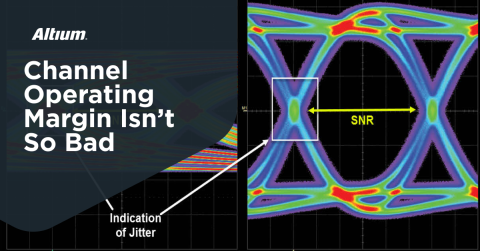
As data streams get faster and rise times get smaller, the above timing window will close, and this puts more emphasis on reducing total jitter that might exist within the timing window. This is one reason we focus on jitter created by power supply noise, ground bounce, and crosstalk in fast interfaces as they also contribute to total jitter.
Angled Routing or Panel Rotation
As was shown in a recent publication in Signal Integrity Journal, routing at a slight angle with respect to the weave pattern can reduce timing skew (standard deviation) from ~7 ps/in. to less than 1 ps/in. Note that this is solely for skew due to the fiber weave effect; other sources of skew like random jitter and delay mismatch in parallel buses or differential pairs still need to be considered. However, angles involved were only ~0.04 rad, equivalent to ~2.3 degrees. In other words, the skew standard deviation can be reduced by approximately 3 ps/degree, up to a maximum reduction of ~7 ps.
Skew reduction Image credit: Bogatin et al. (Signal Integrity Journal).
What this shows is not that skew is eliminated by routing at an angle, just that the standard deviation in timing becomes smaller. This is one reason a board shop may rotate artwork on a panel (maybe 10 degrees) in order to combat fiber weave-induced timing skew. Rather than manually routing or zig-zagging the traces in the PCB, rotating the artwork on the panel allows the designer to work as normal in their PCB design software. The downside is that the artwork on a panel will take up extra space, so it increases per-board fabrication costs.
Spread Glass
Spread glass will flatten out when placed into the PCB stackup, which will ensure fiber bundles fill in the space in the PCB laminate that is occupied by resin. By filling in the resin region with glass, the material appears more homogeneous at practical frequencies used in today's electronics. This minimizes skew between each trace in a differential pair or between single-ended traces in parallel buses.
Set Differential Pair Spacing = Glass Pitch
If the glass weave pitch is known, then this can be used as the spacing between differential pairs. This will ensure that the traces in a pair will always occupy nearly identical weave regions along a straight route, so this will reduce the intra-pair skew. A similar design rule could be used in parallel single-ended buses and parallel differential buses.
Unreinforced Laminates for RF Boards
Another option for advanced RF boards is to use an unreinforced PTFE-based laminate, which will not have a glass weave. The downside of these laminates, aside from the cost, is the fact that they can be difficult to work with in fabrication. Because they have no structural reinforcement, they are sometimes called "wet noodles" as they will easily bend. As a result they might have higher potential for layer-to-layer misregistration. For RF boards used with phased arrays,the elimination of skew on long interconnects is very useful, especially if your system host controller has no mechanism for skew compensation via a power-on calibration procedure.
Periodic Loading at GHz Frequencies
The cavities in loose fiber weaves are essentially partially open resonators, and resonances excited in the fiber weave structure in a PCB material is not defined or observed in simulation or analysis. Remember that the electromagnetic field is not confined within a trace, it exists around the trace and is confined in surrounding medium. This means a travelling high frequency signal, or a digital signal with large bandwidth, can excite one or more resonances in these cavities. These resonances can be approximated as resonances in a rectangular box and we would expect the following set of frequencies:
The lowest order fiber weave resonant frequency is typically ~50 GHz for loose weaves. These resonances can then excite sub-harmonic cavity resonances through resonant coupling. In other words, the fiber weave pockets, nearby conductive structures, and the parasitics created by each act as a source of radiated EMI. This particular issue was recently discussed in Signal Integrity Journal.
Strong resonance in these cavities can also couple inductively or capacitively into nearby circuits. This coupling is more of a problem in RF signal chains involving power amplifiers, high power FET drivers, and similar circuits that produce strong RF fields. This effect appears as a drop in the insertion loss profile at successive fiber weave resonances. You can measure this effect by extracting the S-parameters from a test coupon with a vector network analyzer.
Spectrum analyzer
In summary, if you want to prevent problems with resonances and insertion loss dips, aim for the tightest glass weave style that meets your loss, CTE, Tg, and thermal conductivity requirements. A tighter weave style will generally have higher frequency resonances, although there will be definite tradeoffs that need to be balanced. Accurately accounting for skew and ensuring controlled impedance requires determining the right average dielectric constant to use in your impedance calculations. In the event cavity emissions become problematic, you might consider using a conformal coating as a shielding material.
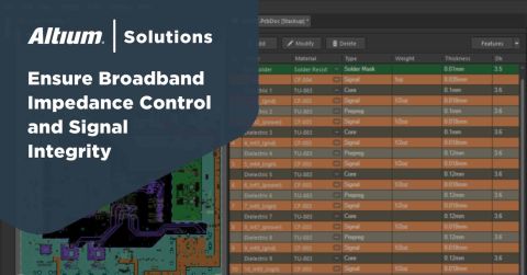
The layer stack manager in Altium Designer® allows you to define the average dielectric constant your signals will see as they travel along a signal trace. This makes it an ideal tool for compensating skew from the fiber weave effect in your board. The post-layout simulation tools are also useful for examining crosstalk between traces carrying high frequency signals and for controlled impedance routing. You’ll have access to an extensive library of standardized materials and weave styles that you can use in your stackup.
Now you can download a free trial of Altium Designer and learn more about the industry’s best layout, simulation, and production planning tools. Talk to an Altium expert today to learn more.


