


Switching Power Supply Output Filter: Design and Simulation

At a Glance
SPICE packages can help you design a switching power supply output filter bby looking at transient response results and running parameter sweeps.


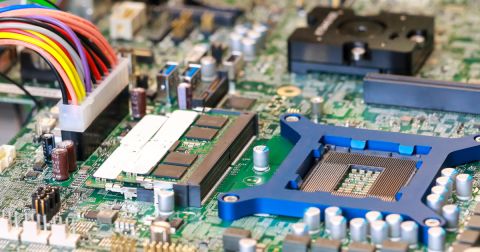
Switching power supplies come in many forms, such as in a high-power benchtop lab power supply, or embedded onto a PCB with specialty ICs and passives. The goal in designing these systems is to ensure stable DC power delivery to the rest of your system with minimal noise. It’s also ideal to dampen the effects of any residual ripple from rectification or remove any noise on the input. Keeping the output noise-free and stable might require using an output filter, which can be implemented using passives in your PCB layout.
In this article, I’ll show how a switching power supply output filter can be used to dampen output noise and how you can use some simulation tools to optimize your filter design for low noise. As I’ve discussed in an earlier article on this blog, and as we’ll see from some simulation results, reducing noise depends on the values of the components in the output filter and the inductor in the circuit. As an example, let’s look at a buck-boost converter topology to see how to implement an output filter for a switching power supply.
Starting a Switching Power Supply Output Filter Design
The output filter on a DC/DC converter (whether buck/boost or other topology) is a low-pass filter. This can be as simple as a shunt capacitor, although the typical method is to place a pi-filter to shunt AC noise to ground. The reason for this is that the function of a switching converter is to exchange low frequency ripple from AC-DC power conversion into higher frequency switching noise from a switching transistor. The output filter then removes the higher frequency switching noise on the output from the filter, giving clean DC power to the load.
The image below shows a switching buck-boost converter schematic with a power PMOS transistor (you could use NMOS and change the V1 and V2 polarities). I’ve highlighted two sections: the switching converter section (in green) and the output filter section (in red). In this circuit, the output capacitor is part of the switching power supply output filter. The filter has a standard pi-filter topology to provide low-pass filtering.

Finally, we have the following parameters on the PWM: 100 kHz switching frequency, 10 ns rise time, 30% duty cycle. Rather than focusing on the allowed range of PWM or passives values that give a specific power output, we want to focus on the range of filter component values that give us the lowest noise. First, we’ll look at the actual transient response with Altium Designer’s new simulation dashboard feature, then we’ll look at a range of filter component values that give the lowest noise.
Initial Power Output
The image below shows a transient simulation showing the voltage across the capacitors (top graph) and the current delivered to the load (bottom graph). From this result, we can compare the unfiltered output (red curve, top graph) with the filtered output (blue curve, top graph). The filter does a decent job of cleaning up the switching noise from the converter. However, there is a clear low frequency transient response as the converter switches from OFF to ON.

This transient response is very important. In fact, the transient overshoot depends on the rise time of the PWM signal and the parasitics in the MOSFET, as well as the poles present in the filter circuit. In certain cases, the overshoot can reach as high as 50% of the load current when the converter switches between two voltage states, i.e., when switching between two PWM frequencies or duty cycles. This could produce a large current spike that could damage your load.
What Contributes to This Transient Response?
Here, we have multiple contributors to the transient characteristics observed above:
- High frequency ripple as seen in the red curve above
- A mid-range frequency transient response from the LC filter poles
- A lower frequency transient response producing the large overshoot due to transients in the MOSFET.
As we'll see, output filters are really good for dealing with #1 and #2. They are not the best option for dealing with #3, but they will affect the transient response due to the MOSFET's parasitic elements.
The Load Impedance
The value of the load component also influences the ripple on the output in this circuit. In the image below, I’ve shown what happens when the load resistance is increased to 1 MOhm, which is a useful value for simulating the input impedance for a CMOS integrated circuit. From here, we can see the true ripple on the output, which is reflected in the load current.

For this reason, we’d want to dampen the response from the converter circuit, or redesign the filter section so that we do not have such a problem with overshoot on the output. One option is to add some damping directly by adding some resistance.
Adding Resistors for Damping
One way to solve a problem with an underdamped transient response is to add some damping on the capacitors C1 and C2. To do this, I’ve added 1 Ohm resistors to capacitors C1 and C2 in order to provide some damping, and I’m driving the 10 Ohm load. This will bring the transient response very near the critically damped regime, giving a smooth transition between OFF and ON states when the simulation begins. The same smooth transition would occur between two power output states if the PWM parameters were changed. However, if the resistors are larger, we’d have a slower transient response.

One slight problem with this is we’ve lost a small amount of power: we have less current reaching the load and the output voltage is slightly lower. Some of the power is dropped on the resistors in the RC section, leading to some additional losses. There is also some slight leftover noise on the output current as well, although this is very small.
We get the same kind of response if we use the 1 MOhm load, but we see some initial ripple in the voltage drop across C1 + (series resistor) net. This is a decent response as the ripple does not get reflected to the output, but there is still the same slow output current rise. This is okay if you do not need very fast regulation with a feedback loop and you want to ensure smooth transfer between states.

Before going further, I think it’s important to note that, while the response is much slower, we’re resign to ~95% of the expected final current in ~3 ms, which is still a reasonably fast turn-on time. Just for comparison, some commercial power supplies are rated at 10x total turn-on time. This turn-on time could be dominated by other components like the PWM driver, especially if there is a feedback loop to provide precision control. Therefore, we’re still operating sufficiently fast, even though the turn-on time looks very slow.
One option here is to re-engineer our switching power supply output filter circuit without added resistance in order to produce a similar result.
Changing C1, C2, and/or L2
Another option here is to remove the resistors and change C1/C2 and L2. The issue with modifying C1 and C2 is that the end ripple on the output side will be affected by the value of these capacitors as you are modifying the conditions for critical damping. The condition where critical damping arises is a rather complicated quadratic expression, but intuition should be clear here:
- If the capacitor values are too low, we would have a severely underdamped response with high frequency oscillation.
- If the capacitor value is too high, we have a very slow response as the capacitors take a long time to charge up to the required DC level.
You might be wondering; how do we have an underdamped transient response with overshoot in a pi-filter? In reality, we have 2 LC filters with multiple poles in the combined transfer function due to the presence of multiple reactive elements (2 inductors and 2 capacitors). If you look closely at the above results, we can see two transient responses superimposed on each other. These are the switched LC response from L1 and C1 (the standard buck-boost converter response), and the typical RLC response from L2, C2, and the load resistor.
Adjusting L2 and the output capacitors together is another way to get to a low ripple on the output. In the image below, I’ve created a frequency sweep in my Simulation Dashboard in order to move through a range of inductor values. Here, I want to confine myself to practical inductances I’d find in smaller components while driving the 10 Ohm load. To ensure I’m getting as close as possible to critical damping, I’m going to sweep through different values of C1 = C2 and L2. I’m starting with a smaller capacitance (1 uF) and sweeping through values of L2 up to 0.2 mH. For the 1 MOhm load, just follow the same procedure using the conditions for critical damping in an RLC circuit.
As it turns out, the best inductance value for L2 is about 150-200 uH. There are plenty of wirewound inductors with DC current ratings exceeding ~1.5 A. One example is the IHV30EB150 from Vishay.

Summary of Filtering Strategies
What have we learned here? There are a few insights we’ve gained and a few points we can infer from these simulations:
- Your filter design depends heavily on the converter’s output capacitor values. If the output capacitors are too small, then you need to place an additional capacitor in parallel to get the cutoff frequency small enough to provide noise filtering.
- We’ve only looked at an output filter, but placing filtration on the input is often much more effective for reducing total noise. This is basically what you are doing with the output capacitor on a full-wave rectifier: you’re trying to feed stable DC power into the power conversion section of the power supply.
- There is an overshoot in the transient response from the pi-filter that can be quite large. This can be damped in the usual way by placing a resistor in series with capacitors C1 and C2 or by adjusting the value of L2.
- When adding damping, be sure to compare the resistance you need with the ESR value of the capacitors you use. Also note that you slow down the circuit’s response and sacrifice some power.
- Because the current spike at the load during the transient response depends on the PWM parameters, we might also take the approach to determine an allowed range of PWM frequencies/rise times that give sufficiently low noise.
Further Improvements
One final option to keep improving the filter response after redesigning is to use an RC snubber before and after the filter. In fact, the capacitor used on the output will have some ESR, so it will act like a mini RC snubber circuit. One option would be to use controlled-ESR capacitors at those points to provide just the right amount of damping as needed.
The more common location to place a snubber is in a converter with high-side and low-side switching elements. This would be placed across the low-side MOSFET to dampen the MOSFET's transient response and produce a smoother output. An example for a buck is shown in the diagram below, but the same idea applies to any other topology where ringing due to MOSFET switching needs to be reduced. Another prime example is in larger switching converters that use multiple MOSFETs in parallel, which can have the same problems with switching and overshoot.

Finishing Up Your SMPS Schematic
In the above example, we’ve only shown the converter section of an SMPS, and there are other important circuit blocks needed to make an SMPS work. The other sections needed in an SMPS depend on the end application and what level of control or precision is needed in the system. In the above example, we haven’t included some other necessary features:
- PWM generation: To set the output voltage to a specific level for a given PWM frequency, a PWM generator can be used to ensure the output voltage to a desired level. This can be as simple as a VCO circuit, or specialty PWM generator ICs can be used.
- Control loop: Some power supply topologies, such as LLC resonant converters, will need a high current control loop, where the converter output is measured and the PWM duty cycle or frequency is adjusted to maintain the voltage to the desired level. An op-amp with a reference voltage is the simplest way to do this adjustment, or this can be done digitally with an MCU. There are also specialized controller chips you can use.
- User interface: The system may need some way to take user input and apply the PWM duty cycle/frequency required to reach the desired output voltage. The easiest way to do this is with an integrated controller, or if you feel like designing your own control strategy you can implement an application on an MCU.
There are some power supply controller components that will sit in the control loop, measure the output voltage, and adjust the PWM signal based on settings applied over a digital interface (usually I2C) and implemented with an MCU.
Once you’ve finished your SMPS schematic and your switching power supply output filter, you can replace any generic components with real components using the Manufacturer Part Search Panel in Altium Designer®. You can then share your designs with your collaborators and your manufacturer using the Altium 365™ platform.
We have only scratched the surface of what is possible to do with Altium Designer on Altium 365. You can check the product page for a more in-depth feature description or one of the On-Demand Webinars.

About Author
Related Resources
Related Technical Documentation
Table of Contents
Design to Release, Without the Friction
- Keep reviews tied to the right version
- Reduce handoff confusion and rework
- Spot sourcing and release risk earlier
- Work solo, share when needed
Get Started
Thank you, you are now subscribed to updates.

