


Using Draftsman to Create a PCB Fabrication Drawing

At a Glance
Download a PCB fabrication drawing example that shows all the important information you should include in your Draftsman document.


When you need to prepare a new design for manufacturing, one of the important docuements you'll need to produce at scale is a PCB fabrication drawing. This drawing shows all of the important information that workers on the line will need to understand the construction of a PCB. A fabrication drawing does more than show an image or rendering of the fabricated board, it also tells the fabrication house all of the requirements the fabricated PCB must meet in order to be accepted.
The other benefit of a thorough and complete fabrication document is that it helps ensure your board can be produced at multiple manufacturers. By compiling a set of consistent requirements into a single location, you have a set of data you can give to any fabricator so they can quickly quote your board for production.
The Draftsman feature in Altium Designer gives users a quick way to generate these drawings without the need for an external drafting application. The Draftsman tool automatically generates professional drawings with information pulled directly from your PcbDoc file. If you're unsure what you should include in your fabrication drawing, we've prepared a cheat sheet to help you get started. Keep reading to see all the information you can include in your PCB fabrication drawing.
What Goes Into a PCB Fabrication Drawing?
Every PCB fabrication drawing needs to have some basic information that lists the requirements of your finished board. Some of these requirements are related to qualification, such as testing and performance metrics, while others concern physical construction of the PCB. Some of the primary information required to produce a fabrication drawing includes:
- A rendering of each layer in the PCB stackup
- A drill drawing with symbols assigned to each drill hole diameter
- A table showing the PCB stackup, via transitions, material information
- An impedance table that lists any controlled impedance requirements
- A list of PCB fabrication notes
- A summative table providing fabrication and performance requirements
- Callouts with any important fabrication information, such as slots or special instructions
- Title block with company and artist information
Including this information in a fabrication drawing PCB will help ensure your fabricator will have all the information they need to properly fabricate the PCB.
General Description, Stackup Table, Impedance Table
To show some of the important information found in a PCB fabrication drawing, we created an example Draftsman document that highlights the available fabrication and documentation features available in Draftsman. The drawing below shows an example of what might be used as a cover sheet for a longer fabrication drawing PCB. This drawing contains a general description of the PCB, and some of the information a fabrication house might need to prepare to plan processing steps.

An impedance table and the layer stack table are important for high speed PCBs that require controlled impedance verification. The fabrication house will use this information to select materials and verify impedances from a TDR mesurement on a test coupon in the event your desired material set is unavailable or does not produce the required impedance specification. The rest of the specifications in your general description will help plan out the rest of the fabrication and finishing process.
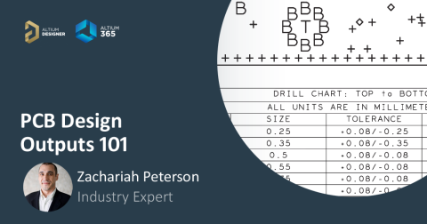
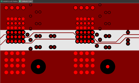
Drill Drawing, Drill Table, Fabrication Notes
The following image shows a typical drill drawing and drill table, which includes drill hole sizes for plated and unplated holes. The finished (plated) hole size will normally include 1 mil plating, so the finished hole diameter will be about 2 mil smaller than value listed in the drill table. This page also contains a complete set of PCB fabrication notes that include important fabrication instructions and requirements. The fabrication notes provide may also include important testing procedures for specialty boards, as well as conformance requirements to relevant industry standards for the finished product.

Gerber Layer Artwork
The final image shown below shows an etch configuration for each layer. In drafting applications, these layers would normally be imported into a drawing from DXF files or Gerber files. If these layers are not exported correctly into a DXF format, there can be incorrect scaling or other drawing errors that cause the draft to have incorrect or missing etch information. Due to the very complex structure of etched layers in a PCB, the layers in the fabrication drawing, the Gerber files, and the PCB layout have to be compared in order to catch any errors. This is very time consuming and
Instead of exporting DXF files or Gerbers, and then re-importing these into your drafting application, Draftsman will generate the drawing shown below automatically using the data from your PcbDoc file. Simply right-click anywhere in the document and select Place Fabrication View from the dropdown menu. The placed fabrication view can then be edited to select the desired scale and layer. The best practice is to arrnage these layres in a single page so that the fabrication team can check the panel order against the etch data in the fabrication view.

A Draftsman document brings an elegant, yet powerful solution for creating fully customizable fabrication drawing PCBs quickly and easily. Everything you need for creating your PCB fabrication drawing - including PCB parameters, drilling and impedance tables, and PCB stackup layers - can be placed in a matter of minutes.
When you’re ready to streamline your design and production workflow, use the world-class CAD features and automated PCB assembly drawing tools in Altium Designer®. You and your team can create advanced designs and quickly prepare them for manufacturing while staying productive and efficient. When it's time to release your designs to production, use the complete set of release management features in the Altium 365™ platform to collaborate with your manufacturer. Everything you need to design and produce advanced electronics can be found in one software package.
We have only scratched the surface of what is possible to do with Altium Designer on Altium 365. Start your free trial of Altium Designer + Altium 365 today.

About Author
Related Resources
Related Technical Documentation
Table of Contents
Design to Release, Without the Friction
- Keep reviews tied to the right version
- Reduce handoff confusion and rework
- Spot sourcing and release risk earlier
- Work solo, share when needed
Get Started
Thank you, you are now subscribed to updates.

