


What Are Netlists in PCB Design Projects?

At a Glance
Your CAD system should not force you to manually work with netlists. Instead, learn about netlists and how advanced CAD systems automate their usage in PCB design, layout, and testing.


Operating behind the scenes of your ECAD software and PCB layout editor is an important dataset that defines the connections between components. This dataset, typically stored in a single file, is known as a netlist. Different CAD systems have different netlist formats, but they play an important function in PCB design software: defining connectivity between components.
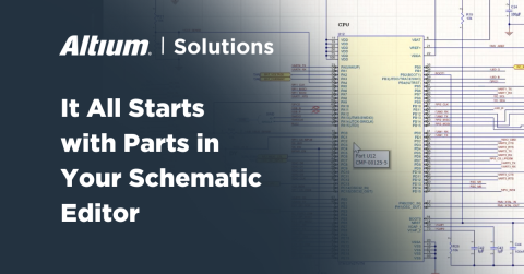
Netlists Start in the Schematic
All netlists are defined at the circuit level and are constructed by CAD tools from circuit diagrams in schematic sheets. A schematic editor will create netlists as you place components and draw circuits, either automatically or with a manual compiler tool. The netlist can then be used in other CAD systems, such as in a SPICE simulation program or a PCB editor. According to an old document from Agilent, early microwave CAD tools and simulators also used their own netlists to perform linear microwave circuit analysis with S-parameters.
No matter how a netlist is used, it will contain a set of human-readable data that follows a specific format. Technically, the entire set of circuits could be reconstructed graphically from a netlist as long as schematic symbols are available, although this is typically done when converting file formats between CAD systems.

Because all netlists define electrical connections between components, they are created from circuit drawing tools or schematic capture programs. Schematic netlists used in PCB design software, whether in Altium Designer or another PCB CAD tool, are then used to define the connectivity between component pads in a PCB layout.
Types of Netlists
Because netlists start in the schematic, they resemble the types of schematics (flat vs. hierarchical) you might see used in PCB projects in ECAD software.
- Flat netlist - This category of netlist simply contains all of the connections implemented in a circuit or design, in contrast to a hierarchical netlist. Most netlists, for example SPICE netlists, will be flat netlists.
- Hierarchical netlist - Also typically referred to in FPGA development, a hierarchical netlilst defines some grouping among nets. In PCB design, nets are normally grouped by schematic, while in FPGAs, nets can be grouped by bank or by the instantiated logic being developed for the target device.
- Schematic netlist - These netlists are exported directly from a schematic capture program and may be converted to a flat netlist, even if the project is hierarchical.
- SPICE netlist - Used in SPICE simulation packages to define electrical connections between internal components or functions that define electrical behavior. These are used to crank numerical calculations and define voltage/current values observed at other nodes in a circuit (See below).
Each of these could be supplied in a vendor-specific format. For example, the SPICE netlist data format used by LTSpice is different from the data format used by PSpice. The same goes for schematic netlists produced by PCB design or schematic capture software. There are also vendor-neutral formats that can be used inside or outside of ECAD software.
Vendor-Neutral Formats
Although a netlist has a specific usage in electronics ECAD programs, CAM software, and EDA software, there is no single file format that is used for netlists. While the data is normally in a human-readable format, the data structure used in netlist files is not standardized across all CAD vendors.
Although the range of netlist formats varies, there are vendor-neutral file formats that can be used to examine connectivity in a design. Some of the most prominent vendor-neutral formats include:
- EDIF (Electronic Data Interchange Format)
- IPC-D-356
- IPC-2581
Uses of Netlists
Once a netlist has been created at a logical level, it can be used in a PCB editor, simulation program, and CAM software.
Airwire (Rats Nest) Construction
Your CAD program can use the textual information in a netlist to determine equivalent connections between pads in a PCB layout. When two pads are assigned to the same net, a PCB editor will use that connection in its design rules to check for opens/shorts, highlight net connectivity, and construct airwires to aid PCB routing.
The PCB layout will contain coordinates and rotation defining component locations and orientation, and the component data will include relative pad locations for each pin appearing in a component’s schematic symbol. Because a netlist defines the connections between each pad in the symbol that same connection data between pads can be used to draw airwires between pads in a PCB editor. This is the basic principle ECAD software uses to display airwires between unconnected nets.
Simulation and Verification
Simulation programs, specifically SPICE simulation engines and specialized circuit simulators (e.g., SiMetrix), will use the circuit connections defined in a netlist to build electrical simulations. The simulator does not necessarily distinguish between different types of components or types of signals (analog vs. digital) when using a netlist to build and run a simulation. Instead, the information in the netlist refers to components, and the simulation model or subcircuit attached to those components is used to execute numerical calculations for a simulation.
Beyond ECAD/EDA Software
Netlists are also used in areas outside of schematic capture and PCB layout, and they may be one of the required file exports from your PCB design software. There are two important areas where netlists are also used:
- PCB manufacturing - As part of a design and engineering review before fabrication/assembly; formats include WireList and Telesis
- FPGA development - Used to define logical functionality at the system level based on logic gate connection; formats include Verilog and EDIF
In FPGA development, the Verilog/VHDL format can express much more than simply connections between nodes in circuits. In PCB manufacturing, their usage is also much further from electronics design, focusing more on verifying connectivity in tooling as it is expressed logically in design files.
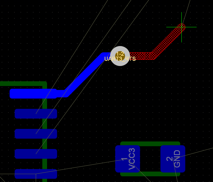
Take the netlist verification shown below as an example. A CAM software package is being used to check that the connections inferred from a Gerber export match the connections defined logically in the netlist. In this case, there is a short between two differently-named nets; this might not violate the PCB design rules due to some rule being waved or overridden, but this type of mistake can be caught in CAM software.

CAM software can use a netlist output to verify that logical connections defined in a netlist match the actual connections in the fabrication data (Gerbers, ODB++) that will be used to produce a PCB. ODB++ exports will include a netlist that is required for this verification and for automated testing (such as with flying probes). When Gerbers are being used, an IPC-D-356 netlist, WireList, or other format can be used to verify connections in the fabrication files.
When you want a high-efficiency ECAD software package that automatically synchronizes your PCB layout and schematics, use the complete set of CAD utilities in Altium Designer®. When you’ve finished your design, and you want to release files to your manufacturer, the Altium 365™ platform makes it easy to collaborate and share your projects.
We have only scratched the surface of what’s possible with Altium Designer on Altium 365. Start your free trial of Altium Designer + Altium 365 today.

About Author
Related Resources
Related Technical Documentation
Table of Contents
Design to Release, Without the Friction
- Keep reviews tied to the right version
- Reduce handoff confusion and rework
- Spot sourcing and release risk earlier
- Work solo, share when needed
Get Started
Thank you, you are now subscribed to updates.

