


5 Power Integrity Myths: AC Edition

At a Glance
Power integrity comes in two flavors: AC and DC. Don’t let yourself be fooled by these 5 myths in AC power integrity.


If you thought signal integrity and EMI were fraught with myths, then wait till you meet power integrity. In power electronics and PCB design, power integrity comes in two flavors: we discussed DC power integrity elsewhere on the blog, now it's time to look at the five biggest myths in AC power integrity. Let's go ahead and jump right in!
Myth 1: Any Power Supply Will Work
Many discussions on power integrity completely ignore the role of the power regulator and assume that the power regulator is theoretically perfect. In reality, semiconductor manufacturers supply components for high-speed digital systems with purpose-built power regulators to supply power at high speeds. Typical voltage regulator modules for high-speed digital power rails have two important characteristics:
- They are multiphase buck converters
- They have high control loop bandwidth
- They have low output inductance
The reason for the first point is that multiphase designs can run with a higher effective switching frequency at low duty cycle per phase, which reduces switching noise on the output. I’ve described this important point in another blog.
However, for high-speed digital designs, the second point is more important as it determines how fast the regulator can respond to transients on the output and thus maintain a stable output voltage. The corollary to the second point is that the regulator has a low output impedance, and that impedance needs to stay low up to very high frequencies. Together, these factors ensure that the regulator and the structure of the PDN (with its discrete capacitors and plane capacitance) can suppress ripple on the power rail when fast digital I/Os begin switching.
Myth 2: A Single Power Layer Is Acceptable
Some designs can get away with a single power layer, even if it is divided up into multiple rails. For smaller digital processors, which might have less than 1000 balls in a BGA package, there will still be multiple supply voltages required. However, the power layer could be segmented into large rails in order to deliver all the required power to the processor. An example showing the possible number and diversity of power rails on a single layer supplying a large BGA is shown below.
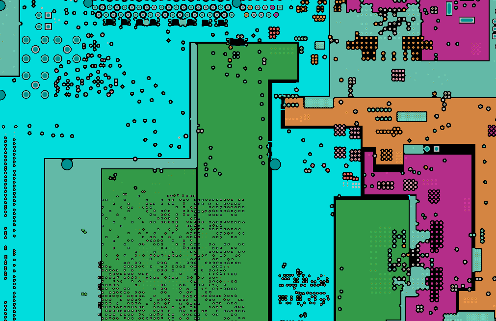
If you attempt to put too many power rails on a single layer, the rails may end up carrying too much current. Instead, you might need another power layer for the high-current rails.
As processors get larger and must support more I/Os at higher speed, multiple power plane layers may be needed, and each of them must have their own ground plane. This is needed to supply enough plane capacitance to keep the PDN impedance below a suitable target. Sub-mOhm PDN impedances into the 100 MHz to 1 GHz range are the norm with large digital processors. Examples of such processors include large CPUs and large FPGAs with more than 1,000 pins.
Myth 3: Low-Dk Dielectrics Are Good for Power Integrity
High-speed digital designs often use advanced FR4 materials with Dk values between 3 and 4. These materials also tend to have low dispersion, and when coupled with the low Dk value, these materials are beneficial for signal integrity in high bandwidth channels. However, low Dk dielectrics are not always the best option for power integrity.
It’s not that low-Dk materials are “bad” for power integrity, rather that a higher Dk value in the power-ground plane pair can be a better option. The reason is that higher Dk dielectrics provide greater plane capacitance for a given thickness. This is why, in some cases, a stackup will use a specialty material known as an embedded capacitance material (ECM). These materials tend to have three important properties:
- Very small layer thickness values
- Very high Dk value
- Higher Df value than advanced FR4 materials
The higher Df value helps dampen transients at high frequency, while the high Dk value and low layer thickness help provide very high plane capacitance reaching into the GHz range. Beyond these frequencies, the processor's in-package PDN impedance will take over and will determine power integrity seen at the bumps on the die.

Data showing decreased PDN impedance when a thinner ECM is used in a PCB stackup. We can very clearly see that the resonant behavior near 1 GHz is greatly decreased through the use of a thinner ECM material. [Source: DuPont]
Myth 4: The Three Capacitor Values
The most common guidance you will find regarding the selection of the decoupling/bypass capacitors is to use three capacitor values separated from each other by a decade, i.e., 10 µF, 1 µF, and 100 nF. This may be fine for ASICs but it can quickly fall apart for large digital processors requiring low PDN impedance with no resonant peaks. This is because the resonances can easily exceed the target impedance value, resulting in strong transients at those frequencies which interfere with power delivery.
The image below from the seminal Signal Integrity Journal article by Eric Bogatin, Steve Sandler, and Larry Smith illustrates why this may not be the optimal selection of capacitors for large digital processors requiring power at high bandwidth.

PDN impedance with multiple MLCC values. [Source: Signal Integrity Journal]
While adding more capacitors will bring down the PDN impedance curve, an extremely large number might be required in order to reduce the PDN impedance peaks below the target impedance value. A better approach is to spread out the capacitor values beyond the three values given in the classic design guidance. This can smooth out the PDN impedance peaks, resulting in a lower number of total capacitors needed to keep the impedance curve below the target value.
Myth 5: Capacitors Must Always Be Close to the VDD/GND Pins
For smaller processors in quad packages and ASICs, this statement is actually true, particularly when power is not delivered with a power/ground plane pair. But in larger digital processors in BGA packages, which require power-ground plane pairs to reach the pins in the inner package region, it is not possible to place all the capacitors close to the power and ground pins.
When power-ground plane pairs are used in a design with a BGA, the path inductance through the plane is far lower than the inductance of any connection routed with traces and vias. A power/ground plane pair behaves as a distributed low-inductance structure, typically in the range of 0.1 to 0.5 nH, whereas a short trace and via combination introduces 1 to 2 nH, and longer trace paths with multiple vias can reach 5 to 10 nH or more.
The table below shows example inductance values for different connection types to illustrate why plane-based routing changes the placement constraint.
Connection Type | Path Inductance Range |
|---|---|
Power/ground plane pair | 0.5 to 1.0 nH |
Short trace with single via | 1 to 2 nH (dominated by vias and ESL) |
Long trace with multiple vias | 5 to 10 nH/inch |
Because the plane pair keeps the interconnect inductance low regardless of the lateral distance between a decoupling capacitor and the processor pins, capacitors placed several millimeters away from the BGA field can still deliver charge effectively during transient events. The governing constraint is not proximity in absolute terms but the inductance of the current path, and plane-based delivery keeps that inductance well below what trace-routed connections can achieve.
Whether you need to build reliable power electronics or advanced digital systems, use Altium’s complete set of PCB design features and world-class CAD tools. Altium provides the world’s premier electronic product development platform, complete with the industry’s best PCB design tools and cross-disciplinary collaboration features for advanced design teams. Contact an expert at Altium today!

About Author
Related Resources
Related Technical Documentation
Table of Contents
Design to Release, Without the Friction
- Keep reviews tied to the right version
- Reduce handoff confusion and rework
- Spot sourcing and release risk earlier
- Work solo, share when needed
Get Started
Thank you, you are now subscribed to updates.

