


Flexible Circuits in Assembly: What PCB Designers Don’t See Until It’s Too Late

At a Glance
Learn flexible circuits assembly challenges in real production. Discover how design decisions impact yield, placement, and reflow performance.


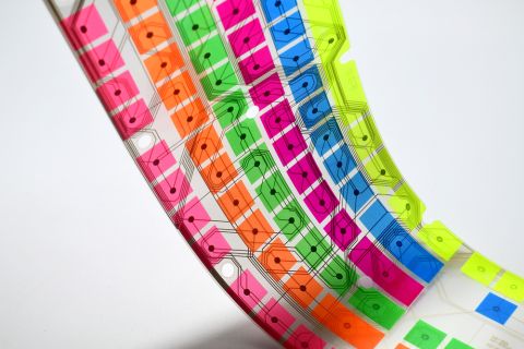
Flexible circuit designs can reduce connectors, enable folding, bending, and creative packaging that rigid boards simply cannot support. And flex designs can also be challenging on an assembly line. Features that looked clean in CAD can be the same ones slowing placement or complicating printing.
Flexible circuits behave very differently than rigid boards, even when the layout technically follows every rule, and fabrication and assembly processes need to be adjusted. The differences can often be minor. A panel that no longer sits perfectly flat, or a part that shifts just enough during reflow to raise an eyebrow at inspection. These small behaviors add up quickly once solder paste, placement forces, and heat enter the picture.
These assembly challenges can sometimes surprise a designer. What PCB designers can do to avoid yield loss, rework, and uncomfortable phone calls later?
Key Takeaways
- Flex behavior impacts assembly stability. Flexible circuits are not inherently flat or stable, which can lead to movement, misalignment, and defects during printing, placement, and reflow.
- Design features directly affect manufacturability. Elements like stiffeners, adhesives, and layout decisions can either improve assembly precision or introduce distortion and yield issues.
- Component placement requires different rules. Placement near bend areas, uneven distribution, or heavy components can cause failures during assembly or in real-world use.
- Early collaboration is critical to avoid downstream issues. Many assembly challenges (panelization, thermal behavior, inspection) can only be effectively addressed during design, not after production begins.
Movement During Assembly
Assembly processes rely on panel stability. With rigid boards, it is assumed. With flexible materials, it often has to be engineered in.
A thin polyimide panel may stretch during handling, shift under vacuum pickup, then sag slightly once it hits the conveyor. Even minor changes in tension can affect registration during printing and placement.
In the real world, a flex circuit is rarely perfectly flat unless it is intentionally designed to be that way during assembly. Without support, flex can lift during stencil release, skew during placement, or distort during reflow. Even small shifts can cause significant issues when assembling fine-pitch components.
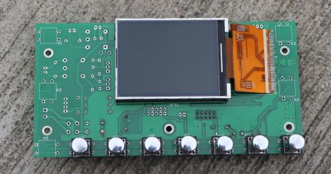
Stiffeners are Process Tools
Stiffeners are often recommended and added to support connectors or specific component areas. Those same stiffeners can be viewed as fundamental tooling during assembly.
A well-designed stiffener creates a predictable, repeatable platform for printing and placement. A poorly designed one creates shadows, uneven pressure, and tilt that no amount of process tuning can fully correct.
Thickness, placement, and even adhesive selection matters more than many designers expect. Some adhesives can introduce uneven expansion, while others soften too early in reflow. Both situations can cause coplanarity issues that show up as opens or weak joints.
When stiffeners are poorly defined or added late, they tend to drive more process adjustments than expected.
Component Placement Rules Change on Flex
Component placement on flexible materials has different considerations than component placement on rigid materials. Components placed too close to bend areas may solder fine initially, then fail after forming or in use. Heavy components can amplify movement during reflow, pulling against molten solder. Dense clustering on one side of the flex can introduce localized warpage that shifts neighboring parts.
Bend areas, transitions, and dynamic flex zones are often where placement assumptions start to break down. Flex relies on balance and symmetry in the stack up to reduce stress and thoughtful spacing improves yield.
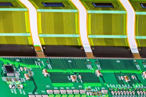
Flex Circuits Need Panelization Too
Flexible circuit panelization requires much more thought than rigid PCBs do. Flexible circuits are often unusual shapes and sizes and also require much more consideration for both fabrication and assembly.
Assemblers often rely on carriers, frames, or temporary stiffeners to move flex circuits through SMT equipment. Breakaway tabs, adhesive carriers, or rigid frames may all be required. Each approach has tradeoffs in cost, throughput, and risk.
Assemblers are forced to work around constraints that may have been avoided with early collaboration, throughput drops, and handling risk increases. By the time panelization becomes a problem on the assembly line, most of the design choices that caused it are already locked in.
Reflow Profiles for Flex PCBs
Flexible circuit materials respond to heat quickly, sometimes too quickly.
Thin polyimide is a great thermal resource. It heats and cools faster than rigid materials and adhesives, coverlays, and stiffeners all influence thermal behavior in different ways. What looks like a standard profile on paper can create distortion, component shift, or uneven wetting in practice.
Assemblers often need tighter process windows for flex builds. Stack up choices, adhesives, and copper distribution all matter. When designers share complete stack up information and material choices early, assemblers can tune profiles proactively rather than reacting to defects after the fact.
Inspection and Rework Are More Difficult
Assembly does not end at soldering. Flex circuits are harder to fixture for AOI. X-ray alignment can be challenging. Manual handling during inspection introduces risk. Rework concentrates heat and stress into already sensitive areas.
Every rework cycle increases the chance of damage. Every inspection step takes longer. These realities influence yield, cost, and delivery schedules. Inspectability and rework tend to get discussed most after something goes wrong.
It is important to remember that early conversation and collaboration between the design and assembly teams can have a significant impact on first pass success. This easy step gives the opportunity for discussion about the various trade-offs that are specific to a particular design and use-case.
Many flex assembly challenges are not process issues, but are the result of design decisions made before fabrication begins. Altium Develop helps engineers keep layout, stackup, and manufacturability considerations visible and connected early, so risks like panel instability, component shift, and thermal distortion can be addressed before they impact yield. By aligning design intent with real‑world assembly behavior, you can move from design to production with fewer surprises and less rework. Get started with Altium Develop →
Frequently Asked Questions about Flexible Circuits in Assembly
1. Why are flexible PCBs harder to assemble than rigid boards?
Flexible PCBs lack inherent rigidity, which makes them prone to movement, stretching, and misalignment during printing, placement, and reflow. Unlike rigid boards, stability must be engineered using stiffeners, carriers, or panelization strategies to maintain accuracy during assembly.
2. What causes component misalignment on flex circuits during reflow?
Component shift is often caused by material movement, uneven heating, or poor mechanical support. Thin substrates, adhesive behavior, and copper distribution can all influence how the board expands or deforms, leading to misalignment or weak solder joints.
3. How should component placement be adjusted for flexible PCBs?
Components should be kept away from bend areas and distributed evenly to avoid stress concentration and warpage. Heavy components and dense clustering can amplify movement during assembly and increase the risk of failure both during reflow and in final use.
4. How can PCB designers reduce flex circuit assembly issues early in the design phase?
Designers can improve outcomes by factoring in manufacturability from the start, defining stiffeners, panelization, and stackup early, and collaborating closely with assembly teams. Sharing detailed material and layout information upfront allows assembly processes to be optimized before production begins.
About Author
Related Resources
Related Technical Documentation
Table of Contents
Design to Release, Without the Friction
- Keep reviews tied to the right version
- Reduce handoff confusion and rework
- Spot sourcing and release risk earlier
- Work solo, share when needed
Get Started
Thank you, you are now subscribed to updates.