






Design for PCB Inspection in Ultra HDI

At a Glance
Verify ultra HDI boards with confidence through design-for-inspection practices. Learn how pad geometry, spacing, and AOI setup ensure PCB quality at high-density scales.


I was sitting in on an ultra HDI design review meeting a while back when someone asked the question that probably should have opened the meeting: "Once this thing is built, how do we actually know it's good?" The room got quiet in that particular way that means the answer is more complicated than anyone wants to admit.
That question, how do we know it was built right is one of the most important ones you can ask on an Ultra HDI program.
A fabricator I work with put it simply a while back: "We can build it. The real question is whether we can verify it." That comment has stuck with me, because it gets at something that does not always make it into the design conversation early enough – inspection strategy.
In Ultra HDI, the ability to confirm build quality is not just a manufacturing detail. It is part of what makes the technology usable at production scale and designers who understand that from the start are in a much stronger position than those who discover it after the first build.
Key Takeaways
- Inspection strategy belongs in early design. Build quality verification cannot be an afterthought. Designers who engage fabricators on inspection capability from the start avoid costly surprises and rework after manufacturing.
- Design decisions drive inspection success. Pad geometry, spacing, and soldermask choices directly influence how effectively AOI and optical inspection tools can evaluate the board. At Ultra HDI scales, these effects are amplified.
- Plan X-Ray inspection upfront. Fine-pitch BGAs, stacked microvias, and buried structures require X-ray evaluation. Treating X-ray as a planned part of the inspection strategy simplifies program planning and cycle time estimation.
- Inspection confidence enables manufacturing scale. A PCB that performs electrically and can be reliably verified at volume is what unlocks true manufacturing scalability. Design-for-inspection is how that confidence gets built into the process.
Smaller Features, Sharper Focus
PCB inspection has always been about clarity, relying on clear separation between features, strong visual contrast, and enough access to evaluate what is happening without ambiguity. Ultra HDI changes that environment; pads are smaller, spacing is tighter, and components are closer together.
What used to be visually obvious now requires a more refined approach to evaluate.
One of the things I find genuinely interesting about Ultra HDI inspection is how it has pushed the industry to get better at it. Long before Ultra HDI technology, we have been dealing with tighter and tighter geometries that have driven meaningful advances in AOI programming, lighting technology, and system calibration. Equipment that would have struggled with sub-50-micron features just a few years ago is now purpose-built for them.
Inspection capability has grown alongside fabrication capability. Understanding that context helps set realistic expectations. AOI at Ultra HDI geometries requires more precise tuning, tighter calibration, and deliberate programming. Fabricators who specialize in this work have invested in exactly that. When you are selecting a partner for an Ultra HDI program, their inspection infrastructure is as worth asking about as is their laser drill capability.
What Design Gives the Inspector
Here is something that does not always get discussed clearly: design decisions directly influence how effectively inspection tools can do their job.
- Visual separation between features matters.
- Soldermask geometry affects how clearly adjacent pads can be distinguished and pad sizing.
- Spacing influences whether a borderline condition reads as a pass or triggers a review.
None of this is new. It applies in standard PCB design too. But at Ultra HDI scales, the effect is amplified.
This is one area where engaging your fabricator early can really pay off. They can tell you where inspection tends to get complicated on a design and how layout choices can make verification more straightforward.
When X-Ray Is Part of the Plan
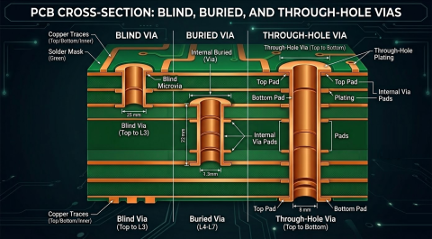
Fine-pitch BGAs, stacked microvias, and buried interconnect structures are exactly what make Ultra HDI designs so capable for complex, dense designs. They are also features that require X-ray inspection rather than optical evaluation.
X-ray inspection has become increasingly sophisticated, and the interpretive expertise around it has necessarily grown to match. Fabricators doing Ultra HDI volume have this capability and use it routinely.
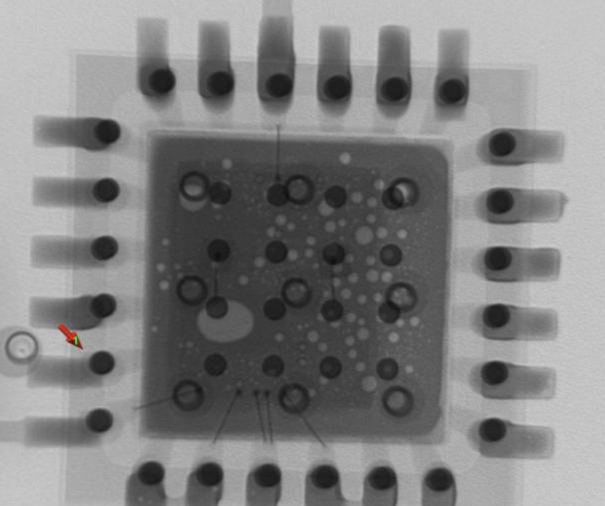
X-ray inspection of a fine-pitch QFN package. Note the wire bonds in the image, as well as the voiding in the die-attached pad in the center.
What matters from the design side is treating X-ray as a thought-through part of the inspection plan, not a fallback. If a significant portion of a design depends on buried or stacked structures, understanding upfront how those will be evaluated and what the expected cycle time looks like makes program planning much cleaner.
Inspection Confidence Is a Deliverable
One of the things I have come to believe strongly about Ultra HDI is that inspection confidence is part of what technology delivers. A printed circuit board that performs well electrically is a critical part of the design process, and a circuit board that can be evaluated with high confidence, every time, at volume, is what makes that performance scalable.
Designing with inspection in mind is part of how that confidence gets built into the process. It does not require pulling back from density. It means understanding how the board will be evaluated and giving the inspection process what it needs to do its job well.
The designers I see navigate Ultra HDI most effectively are the ones who ask early: "How will this be verified?" Not because they are worried about failure, but because they understand that verification is the final step in proving the design works and they want that step to go smoothly.
Ultra HDI is genuinely expanding what is achievable in printed circuit board design. Getting inspection right is part of realizing that potential fully.
Design for Inspection Starts with Design Clarity
Designing for inspectability requires knowing the rules as well as clear communication between design intent and manufacturing reality. Altium Develop gives you the tools to document design decisions, capture fabricator feedback, and maintain version clarity throughout your Ultra HDI program. With built-in design review capabilities and a straightforward path from schematic to release, Develop helps you catch inspection risks early and keep your design team aligned with fabrication partners on what matters: getting the board right the first time.
Learn more about Altium Develop →
Frequently Asked Questions
When should you involve your fabricator in Ultra HDI inspection planning?
Involve your fabricator during design concept or early schematic phase, not after layout is complete. This is when you can ask critical questions about their AOI capability, X-ray equipment, and how your design choices (pad spacing, soldermask geometry, layer stackup) will affect verification strategy. Waiting until design review or manufacturing handoff means you'll discover inspection bottlenecks too late to address them without rework or schedule delay.
How do pad geometry and spacing decisions affect inspection results?
Smaller pads and tighter spacing make adjacent features harder for AOI equipment to distinguish, which can trigger false calls or require manual review. Visual separation between pads, consistent soldermask margins, and deliberate spacing choices directly influence whether a design passes automated inspection on the first run or requires secondary review. At Ultra HDI scales, the effect is amplified, sub-50-micron geometry requires precision tuning that simpler designs don't demand.
What's the difference between optical AOI and X-ray inspection, and when do you need X-ray?
Optical inspection (AOI) evaluates surface features like pad size, soldermask coverage, and component placement. X-ray is required for buried structures: stacked microvias, buried vias, fine-pitch BGA connections, and internal interconnects that optical tools cannot see. If your design uses these features, plan X-ray as a deliberate part of your inspection strategy and include cycle time estimates in your program schedule.
Does designing for inspection add cost or delay to Ultra HDI programs?
No, designing with inspection in mind prevents cost and delay. Early fabricator engagement identifies inspection risks before layout, allowing you to adjust design choices (spacing, pad sizing, layer stackup) at minimal cost. Discovering inspection problems after manufacturing triggers rework, scrap, and schedule slip. Inspection confidence built into the design process is what makes manufacturing scale economically viable.

About Author
Related Resources
Related Technical Documentation
Table of Contents
- Key Takeaways
- Smaller Features, Sharper Focus
- What Design Gives the Inspector
- When X-Ray Is Part of the Plan
- Inspection Confidence Is a Deliverable
- Design for Inspection Starts with Design Clarity
- Frequently Asked Questions
- When should you involve your fabricator in Ultra HDI inspection planning?
- How do pad geometry and spacing decisions affect inspection results?
- What's the difference between optical AOI and X-ray inspection, and when do you need X-ray?
- Does designing for inspection add cost or delay to Ultra HDI programs?
Solutions for Every Role and Team
- Discover and evaluate design options earlier
- Develop in one shared workspace
- Scale with control and compliance
- Connect every stage of hardware development
Learn More
Thank you, you are now subscribed to updates.