


HDI vs. Ultra HDI: What PCB Designers Must Be Aware of on the Fab Floor

At a Glance
Discover how Ultra HDI reshapes PCB design and manufacturing with new process limits, material challenges, and stricter requirements for reliable production.


HDI (High Density Interconnect) technology has been a staple in high-density PCB design and fabrication for years. Most designers are familiar with microvias, sequential lamination, and the trace and space limitations of subtractive etch processing for PCB fabrication. What once seemed like a steep learning curve for both designers and fabricators is now a matter of execution versus process development.
Today, “Ultra HDI” is emerging as a new paradigm in ultra-fine PCB fabrication and advanced interconnect design, with a steep learning curve for both designers and fabricators. At first glance, it may seem that Ultra HDI is simply an evolution of HDI technology.
Ultra HDI differs from standard HDI not just in feature size, but in manufacturing approach. While HDI relies on mature subtractive etch processes and well-understood microvia structures, Ultra HDI requires semi-additive copper processes, tighter material control, and significantly reduced tolerance for variation to achieve repeatable production yield.
However, coming from the fabrication floor, Ultra HDI is by no means simply the next generation of HDI processes. It is a new and distinct operating paradigm with new process boundaries, material, and risk considerations entirely. While you can mix Ultra HDI layers and HDI layers into the same stack-up, using Ultra HDI successfully requires advanced knowledge of the processes and process parameters.
Let’s take a practical look at what really distinguishes HDI from Ultra HDI once you go into production with your design.
Key Takeaways
- Ultra HDI introduces a new manufacturing paradigm, where traditional HDI methods (subtractive etch, standard solder mask, basic microvia stacks) become unstable and insufficient at ultra‑fine geometries.
- Reliable production defines success, as UHDI demands semi‑additive copper processes, tighter tolerance control, and far deeper dependency on repeatability across entire panels and lots.
- Materials and registration become primary yield limiters, with glass weave, Z‑axis expansion, copper roughness, and cumulative dimensional drift directly impacting alignment, impedance, microvia reliability, and overall manufacturability.
- Assembly interfaces impose stricter constraints, often requiring dry‑film solder mask, carefully selected surface finishes, and early collaboration with fabricators to mitigate risks tied to microvia stacking, pad definition, and fine‑pitch soldering.
How fabricators differentiate HDI vs. Ultra HDI in production
In fabrication terms, HDI is still closely tied to conventional multilayer processing. The features are smaller, and the tolerances are tighter, but many of the core methods remain familiar. Subtractive etching, laser-drilled microvias, and standard LPI solder mask can still get the job done when used carefully.
With Ultra HDI, feature sizes shrink to the point that traditional processes become unstable, registration margins disappear, and materials that behave well at HDI dimensions begin to work against you. At that scale, success depends less on whether a rule can be met once and more on whether it can be repeated across an entire panel, lot after lot. Fabrication processes need to make a distinct change to enable fabricators to build product reliability.
Feature Size and Patterning Reality
Most HDI designs operate within trace and space dimensions that are well-established in conventional PCB fabrication processes, utilizing mature processes, predictable yields, and proven inspection methods. However, Ultra HDI technology pushes these feature sizes into a more challenging realm where traditional subtractive etching struggles to maintain consistency due to increased sensitivity to factors like copper thickness variation, etch factor, and imaging accuracy.
- HDI: Utilizes mature, stable processes with predictable yields.
- Ultra HDI: Requires processes like semi-additive or modified semi-additive to build copper features due to the limitations of subtractive etching at extremely small feature sizes.
- Minimum design rules are not the same as stable production capability; DFM checks do not guarantee repeatable yield in Ultra HDI.
For PCB designers, the critical message is that minimum design rules, even if they pass a DFM check, do not guarantee a repeatable and stable production yield in Ultra HDI. Fabricators stress that reliable production capability is distinct from the absolute minimum a rule allows, and designers should prioritize understanding how a feature will be manufactured over simply how small it can theoretically be.
Via Structures: Familiar Shapes, New Consequences
HDI designers should already be comfortable with microvias, often staggered and sometimes stacked one or two layers deep. Reliability at that level is well characterized, especially when materials and plating processes are well matched.
Ultra HDI relies far more heavily on stacked microvias, frequently copper-filled and extending across more than 2 build-up layers. The aspect ratios tighten, plating uniformity becomes critical, and even minor voids can compromise reliability. At these scales, via geometry, fill chemistry, and thermal behavior are inseparable.
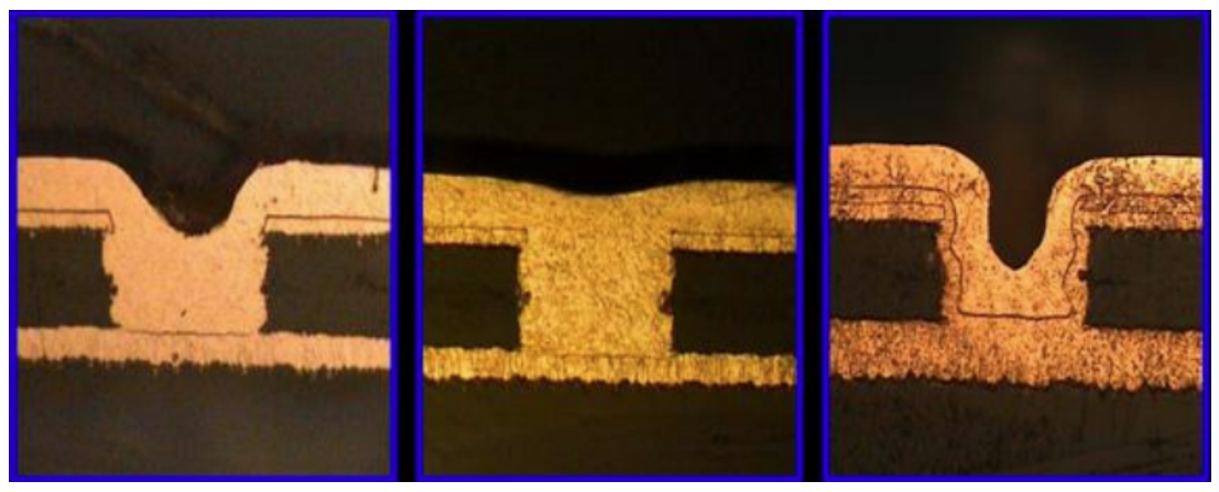
From the fabrication side, deeper stacks increase drill sensitivity, plating complexity, and inspection difficulty. From the design side, every additional stacked layer increases risk of microvia failure during assembly or operation in the field. The question shifts from “Can this be built?” to “Can this survive reflow and field conditions consistently?”
Materials: Constraints and Selection in Ultra HDI
In Ultra HDI designs, material selection establishes the limits of fine-line PCB manufacturing performance, including feature size, registration tolerance, and interconnect reliability. Laminates and copper foils that are acceptable in conventional HDI often become yield-limiting as trace widths, capture pads, and microvia diameters shrink into the tens of microns. At this scale, dimensional stability and surface characteristics dominate over nominal electrical performance.
Several material-related effects must be explicitly accounted for during stackup and layout definition:
- Glass weave non-uniformity introduces localized dimensional distortion and dielectric variation that directly affects impedance control and feature alignment at ultra-fine geometries.
- Z-axis expansion accumulates across sequential lamination cycles, increasing mechanical strain in stacked or closely spaced microvias.
- Copper surface roughness alters effective conductor width and line edge definition when very low copper weights are used, increasing variability in impedance and etch fidelity.
Ultra HDI-capable material systems mitigate these effects through tighter glass control, higher Tg values to reduce thermally induced movement, and very smooth or reverse-treated copper foils. These materials define achievable geometry and registration limits and therefore must be selected before finalizing trace widths, via structures, and lamination strategy.
Registration: Managing Cumulative Dimensional Error
Registration becomes a primary design risk in Ultra HDI layouts due to the limited overlap margin between vias, pads, and traces. Each lamination and imaging step introduces dimensional movement, and the resulting error is cumulative rather than random. In contrast to standard HDI, there is often insufficient margin to absorb these shifts through pad enlargement or spacing increases.
Laser drilling positional accuracy does not eliminate registration risk, as drill placement follows the dimensional state of the material at the time of processing. Photo tooling stretch, core relaxation, and resin flow all contribute to misalignment between layers. When capture pads and trace features are defined at micron-level dimensions, even tightly controlled fabrication processes can exceed allowable tolerance.
Designers directly influence registration robustness through layout structure. Reducing the number of lamination cycles, limiting via stacking, and maintaining consistent alignment of critical features across layers lowers sensitivity to dimensional drift. Allowing realistic spacing between adjacent structures provides tolerance for unavoidable material movement without compromising yield.
Solder Mask and Surface Finish Limits
Ultra HDI pad geometries frequently exceed the resolution limits of traditional liquid photoimageable solder masks. As pad openings shrink and mask dams narrow, thickness control and edge definition become critical to assembly yield. Variability that is acceptable at larger scales becomes a dominant defect mechanism at fine pitch.
In many Ultra HDI applications, dry film solder mask is required to maintain consistent aperture geometry and registration. Mixing solder-mask-defined and non-solder-mask-defined pads at fine pitch increases variability in solder volume and wetting behavior and should be avoided unless explicitly validated with the fabricator and assembler.
Surface finish selection is similarly constrained. Thickness uniformity and deposition consistency have a direct impact on solderability and coplanarity when pads and traces are extremely small. These effects often manifest during assembly and inspection, even though they originate from layout-level decisions.
In Ultra HDI designs, solder mask selection, surface finish, fabrication processes, and assembly requirements are tightly coupled. Choices made during layout propagate downstream with limited opportunity for correction, making early coordination across the manufacturing flow essential.
What Designers Should Do Differently
Designing Ultra HDI successfully requires a mindset shift. Engage fabrication partners earlier than you would for HDI. Ask how features are made, not only whether they pass rules. Build margin wherever the system allows it, even when density pressure is high. Ultra HDI is its own discipline, with its own best practices and failure modes.
Whether you need to build reliable power electronics or advanced digital systems, Altium Develop unites every discipline into one collaborative force. Free from silos. Free from limits. It’s where engineers, designers, and innovators work as one to co-create without constraints. Experience Altium Develop today!
Frequently Asked Questions
What is the main difference between HDI and Ultra HDI?
Ultra HDI goes beyond simply shrinking HDI features, it requires entirely different manufacturing processes, materials, and tolerances. Traditional subtractive etching, standard LPI solder masks, and basic microvia stacking become unstable at ultra‑fine geometries. Instead, Ultra HDI depends on semi‑additive copper processes, extremely tight registration control, and highly specialized materials to maintain reliable yields.
Why can a design pass DFM checks but still fail in Ultra HDI production?
DFM checks verify that a design meets the minimum allowable rules, but Ultra HDI requires repeatability, not just one‑time feasibility. Factors such as material movement, imaging accuracy, copper thickness variation, microvia fill uniformity, and cumulative registration drift can push features outside stable production capabilities. Passing DFM does not guarantee that the design can be manufactured consistently across panels and lots.
How many stacked microvia layers are realistic in Ultra HDI, and what affects their reliability?
Ultra HDI designs commonly require stacked, copper‑filled microvias across multiple build‑up layers, but reliability drops sharply as stack height increases. Aspect ratio, plating chemistry, thermal cycling, Z‑axis expansion, and inspection limits all influence survivability. The key question shifts from “Can it be built?” to “Will it survive reflow and field conditions?”. In practice, reducing stack depth improves yield, reliability, and fabrication stability in Ultra HDI PCB fabrication, where stacked microvia complexity directly impacts process repeatability.
What materials should I choose for stable Ultra HDI performance?
Material choice is one of the biggest determinants of UHDI success. This includes laminates with highly controlled glass weave, low Z‑axis expansion, and very smooth or reverse‑treated copper foils to maintain trace fidelity and registration. These materials help mitigate impedance variation, line‑edge roughness, and dimensional drift that can degrade yields at ultra‑fine geometries.
About Author
Related Resources
Related Technical Documentation
Table of Contents
Design to Release, Without the Friction
- Keep reviews tied to the right version
- Reduce handoff confusion and rework
- Spot sourcing and release risk earlier
- Work solo, share when needed
Get Started
Thank you, you are now subscribed to updates.