
Design lighter, smaller electronics with Ultra HDI PCB technology. See proven SWaP improvements across satellites, wearables, and electric vehicle systems.
Learn about design basics for HDI PCB design. When planning for the HDI PCB manufacturing process, you can prepare accurate designs and deliverables with Altium.
Learn why copper plating for Ultra HDI (UHDI) technology is complex. Discover how design decisions like aspect ratios and stacked microvias impact fabrication reliability and success.
Verify ultra HDI boards with confidence through design-for-inspection practices. Learn how pad geometry, spacing, and AOI setup ensure PCB quality at high-density scales.
Discover how Ultra HDI shifts PCB assembly requirements. Explore stencil design, inspection limits, and rework constraints at fine-pitch BGA layouts.
HDI design and high density interconnect routing require implementing a specific process in the PCB stackup and design rules. Learn more in this chapter of Happy Holden's guidebook.
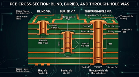
As component density increases, the via strategy usually changes before anything else. Designers can keep shrinking placement spacing and pushing routing into inner layers for a while, but eventually conventional through-hole vias start consuming too much surface area and too many routing channels. That is the point where blind vias start to matter. They are one of several interconnect structures used when package pitch, fanout routing clearance
BGA packages come in multiple pitch values, each of which demands a specific via size for fanout routing on the PCB.
Discover how Ultra HDI reshapes PCB design and manufacturing with new process limits, material challenges, and stricter requirements for reliable production.
View our complete list of resources on usage of blind and buried vias in HDI PCB design.
The PCB is designed and formed as a stack of layers. In the early days of printed circuit board (PCB) manufacturing, the board was simply an insulating core layer clad with a thin layer of copper on one or both sides. Connections are formed in the copper layer(s) as conductive traces by etching away (removing) unwanted copper. Fast forward to today, where almost all PCB designs have multiple…
The traditional approach to circuit board design has been to place the components on the top and bottom surfaces of the board. This process is well supported by circuit board assembly houses, which typically use automated pick and place machines to position each component, ready to be soldered onto the surface. The ever-increasing demand for smaller and more integrated electronic products,…
How many of us got into electronics because we were drawn by the myriad of cool switches, knobs, lights and other suitably gadget-centric controls? Fast forward a good few years and that allure is still there, only it is now replaced with the "Snazzy GUI" factor - electronic products that have a sleek, sexy interface. Central to these ever-advancing (and shrinking) product interfaces is touch…
The Technology Current technologies for fabricating printed electronic circuits include: Laser Direct Structuring - used when fine conductor structures are required. 3d printing - Molding DuPont InMold - a circuit is printed onto a plastic substrate, which is then thermoformed and injection molded into the final product shape. Two shot molding - this is a good approach for large quantities with…
When using a Standalone or Private Server license, you may need to reactivate/refresh that license to be able to access and use the wire bonding functionality. For a Standalone license, this is performed from the License Management view. For a Private Server license hosted in the Altium On-Prem Enterprise Server or Altium Infrastructure Server, this is performed from the Admin – Licenses page of…
Solutions for Every Role and Team
Discover and evaluate design options earlier
Develop in one shared workspace
Scale with control and compliance
Connect every stage of hardware development
Learn More