



Space, Weight, and Power (SWaP) Improvements with Ultra HDI Technology

At a Glance
Design lighter, smaller electronics with Ultra HDI PCB technology. See proven SWaP improvements across satellites, wearables, and electric vehicle systems.


In the world of PCB design, innovation is a necessity. As electronic systems become more compact and power-efficient, engineers face constant challenges in optimizing Space, Weight, and Power (SWaP). That’s where Ultra HDI (UHDI) technology steps in, offering a solution that redefines the limits of PCB design and fabrication.
Key Takeaways
- Ultra HDI maximizes space efficiency through denser routing. By enabling finer line dimensions and advanced microvia techniques (including full-stackup stacked microvias below 4 mil), UHDI allows engineers to pack significantly more circuitry into smaller footprints without expanding physical size.
- Lightweight materials and smarter architecture cut weight meaningfully. UHDI supports thinner layers and advanced materials like polyimide and LCP. Real-world results include a 1.5 kg reduction per satellite unit and a 30% reduction in UAV wiring harness weight; the latter extending flight range by 10%.
- The technology is already delivering results across demanding industries. UHDI is actively in use in CubeSats, smartwatches, and automotive systems. A luxury EV manufacturer reduced its battery management system weight by 12% using UHDI, directly improving vehicle range.
- Early collaboration with fabricators is essential. Design rules for UHDI manufacturability are still rapidly evolving. Engineers are advised to engage with expert fabricators early in the development process to shorten the learning curve and avoid costly design revisions later.
Maximizing Space Efficiency with Ultra HDI
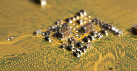
One of the biggest challenges in PCB design is packing more functionality into smaller form factors. Ultra HDI enables this by increasing routing density and introducing advanced interconnect techniques.
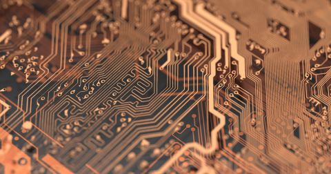
For example, fine-line Ultra HDI PCBs allow for dramatically reduced line and space dimensions, making it possible to fit more complex circuits into smaller footprints. This means that an avionics module, traditionally constrained by space, can now incorporate additional processing power or sensors without expanding its physical size.
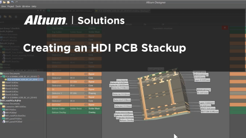
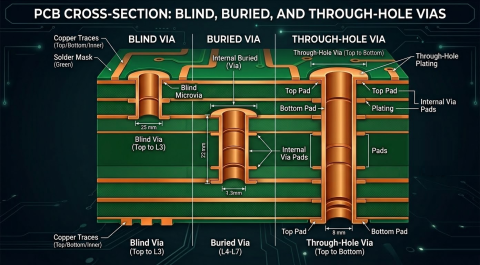
Another aspect of UHDI is the use of microvias with size limits pushed well below what is typically seen in laser drilling (i.e., less than 4 mil). HDI designs can implement larger microvias, which may not always stack through the entire PCB stackup. Ultra HDI designs often implement ELIC through the entire PCB stackup with stacked microvias and buildup films on almost all layers. These devices may even forgo the use of through-holes entirely in favor of full-stackup via stacks of small microvias.
Reducing Weight Without Compromising Performance
Weight reduction is a top priority in industries like aerospace, automotive, and wearable electronics. Ultra HDI technology contributes to this goal by enabling thinner PCB layers and incorporating lightweight materials such as polyimides, Liquid Crystal Polymer (LCP), and a host of advanced, newly developed materials in development today. These materials not only reduce overall weight but also enhance flexibility and durability.
Consider the situation of a satellite integrator that switched to Ultra HDI-based technology and polyimide materials. This transition resulted in a weight reduction of 1.5 kg per unit, which in turn lowered launch costs significantly. When every gram counts in space applications, such savings are game-changing.
Beyond material selection, Ultra HDI also simplifies interconnects by reducing the need for bulky connectors and excessive cabling. In one UAV application, engineers slashed wiring harness weight by 30%, ultimately extending the drone’s flight range by 10%. This demonstrates how optimizing PCB architecture can lead to tangible performance benefits.
Real-World Applications: Ultra HDI in Action
Ultra HDI isn’t just a theoretical breakthrough; it’s actively reshaping industries. Let’s look at some interesting use cases where this technology is delivering tangible results.
Satellites and Spacecraft
In space applications, size and weight constraints are paramount. Ultra HDI enables engineers to design compact payloads without sacrificing functionality. CubeSat programs, for instance, have successfully integrated Ultra HDI technology to accommodate advanced sensors in minimal space. This ensures compliance with strict weight limits while maximizing mission capabilities.
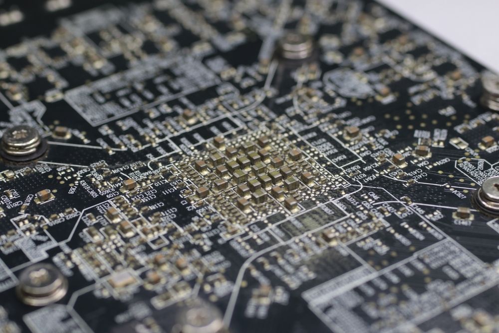
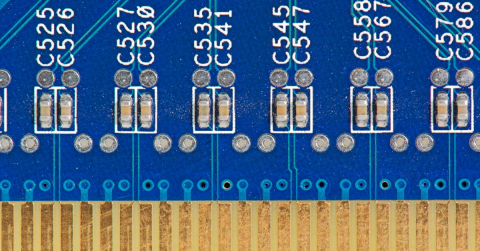
High-density rigid PCB for digital control in SATCOM
Wearable Devices
The demand for sleek, lightweight wearable electronics is always growing. Smartwatches and fitness trackers require high-density PCBs to house multiple sensors and communication modules without increasing thickness. By utilizing Ultra HDI technology, designers have successfully incorporated additional features while keeping devices compact and comfortable for users.
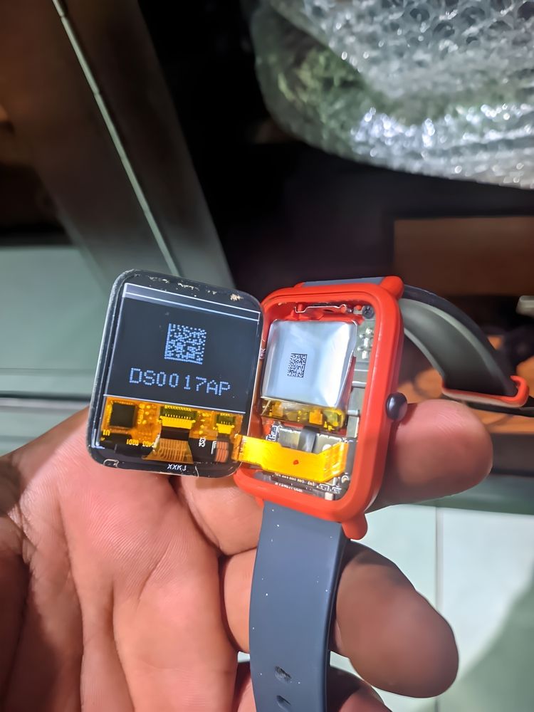
Interior of a smartwatch with high-density flex PCB
Automotive Electronics
The automotive industry, particularly in electric vehicles (EVs) and Advanced Driver Assistance Systems (ADAS), take advantage of Ultra HDI to streamline electronic control units. A luxury EV manufacturer leveraged technology to reduce the weight of its battery management system by 12%, resulting in an extended vehicle range. This demonstrates how improving PCB efficiency can have a direct impact on real-world performance and energy savings.
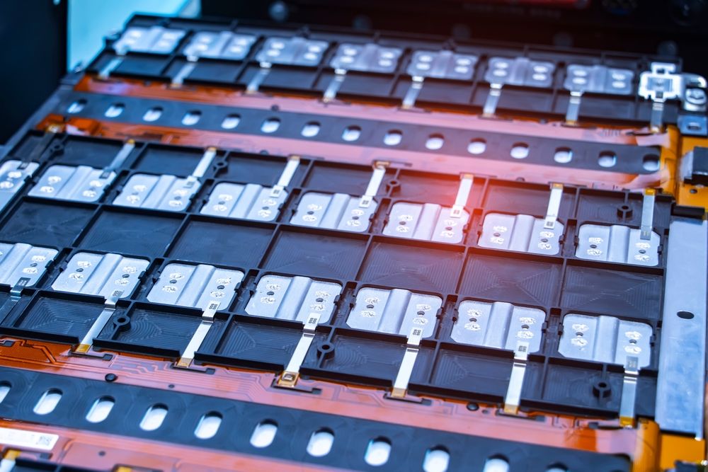
Flex ribbon array in Li battery pack
Why Ultra HDI is the Future of PCB Design
The advantages of Ultra HDI go beyond just space savings, weight reduction, and power efficiency. It enables designers to push the boundaries of what’s possible, integrating more functionality into smaller, lighter, and more efficient electronic systems.
As industries continue to demand higher performance from compact devices, Ultra HDI will play a critical role in meeting those challenges. Whether you’re developing aerospace modules, next-gen consumer electronics, or high-efficiency automotive systems, embracing Ultra HDI could be the key to staying ahead of the competition.
Are you ready to revolutionize your PCB designs with Ultra HDI? Now is the time to explore how this groundbreaking technology can optimize your next project. Step one, research potential fabricators and start the conversation to learn how to best implement this technology in your PCB designs. The design rules and guidelines for manufacturability are developing rapidly. Shorten the learning curve by working with the experts early in your development process.
Ready to design smarter, smaller, and lighter PCBs? Explore how Altium's solutions support your next high-density design →
Frequently Asked Questions
What is the difference between HDI and Ultra HDI (UHDI)?
HDI uses microvias and blind/buried vias to increase routing density, typically working with trace widths down to 3 mils (75 microns). Ultra HDI goes further, achieving sub-1-mil (sub-25 micron) trace widths and spaces that require entirely different fabrication processes, primarily semi-additive processes (SAP or mSAP) rather than traditional subtractive etching. The shift from HDI to UHDI is not incremental; it involves new materials, equipment, chemistry, and inspection methods.
Which industries benefit most from Ultra HDI technology?
Ultra HDI delivers the greatest impact in applications where space, weight, and reliability are non-negotiable. These include aerospace and defense (CubeSats, avionics, UAVs), automotive electronics (EV battery management systems, ADAS), wearable devices (smartwatches, medical implants), and high-speed computing (AI systems, servers, advanced packaging). Any application requiring high component density in a constrained form factor is a strong candidate.
What materials are used in Ultra HDI PCB designs?
Ultra HDI designs rely on advanced laminates with tightly controlled glass weave, low Z-axis expansion, and very smooth or reverse-treated copper foils. Common choices include polyimides and Liquid Crystal Polymer (LCP), which reduce overall board weight while improving flexibility and dimensional stability. Material selection directly determines feature size limits, registration tolerances, and long-term reliability, making it one of the most critical early design decisions.
When should I involve a fabricator in my Ultra HDI project?
Earlier than you would for standard HDI. UHDI design rules for manufacturability are still evolving, and current HDI guidelines such as IPC-2226 do not fully address designs with trace and space dimensions below 50 microns. Engaging a fabricator at the start of the design process, before stackup and routing decisions are finalized, helps avoid costly redesigns and ensures your design stays within verified process capabilities.

About Author
Related Resources
Related Technical Documentation
Table of Contents
Solutions for Every Role and Team
- Discover and evaluate design options earlier
- Develop in one shared workspace
- Scale with control and compliance
- Connect every stage of hardware development
Learn More
Thank you, you are now subscribed to updates.



