







UHDI Copper Plating: What Designers Need to Understand About the Process

At a Glance
Learn why copper plating for Ultra HDI (UHDI) technology is complex. Discover how design decisions like aspect ratios and stacked microvias impact fabrication reliability and success.


The copper plating process that produces vias is very well understood by fabricators and the traditional subtractive etch process for standard technology and High Density Interconnect (HDI) has decades of experience behind the design rules for aspect ratio and design best practices and those rules are well understood by the PCB design community.
On the surface, the copper plating process for Ultra HDI technology shouldn’t be that complicated, right? But, Ultra HDI technology doesn’t have decades of experience behind the process, and the margins and tolerances take on a whole new meaning when feature sizes move below 75 microns, especially when they are near the 25 micron range.
Copper plating in UHDI isn't a background process fabricators handle automatically. It's a set of variables that interact directly with design decisions, and when those variables aren't correctly accounted for, both fabricators and the PCB designer can have several issues to work through during prototyping and development.
Key Takeaways
- UHDI plating is a geometry problem, not just a fabrication one. As via diameters drop below 75 microns, current distribution becomes uneven and copper thickness variation increases, and the geometry driving that risk comes from the design.
- Aspect ratio is the critical number designers control. For laser-drilled microvias in UHDI, staying at or below 1:1 (depth to diameter) is a hard plating physics constraint, not a fabricator preference. There is no margin to push it.
- Stacked microvias require complete, flat copper fill before the next layer can be built. Any dome, recess, or off-center fill becomes a built-in failure point for the via stacked on top of it.
- Electrical test alone won't catch UHDI plating risk. A via can pass continuity and still carry a plating profile that fails under thermal cycling in the field. Cross-section analysis at first article is the only way to know what's actually happening inside the structure.
Why Plating Gets Harder as Features Get Smaller
In standard PCB fabrication, plating is a mature process. The tolerances are understood, the chemistry is dialed in, and fabricators have years of data to draw on. Move into UHDI geometries and a lot of that comfort disappears.
The core issue is access. Electrolytic copper plating deposits copper ions onto conductive surfaces in the presence of an electrical field. At larger geometries, current distributes reasonably evenly. As via diameters drop below 75 microns, that distribution gets harder to control. Current density concentrates at edges and corners. The field inside a small via isn't the same as the field at the surface. Copper builds faster in some areas than others, and thickness variation becomes significant at the feature sizes UHDI demands.
This isn't a fabricator problem that better chemistry solves on its own. It's a geometry problem, and the geometry comes from the design.
Aspect Ratio: The Number That Drives Plating Risk
Aspect ratio (the relationship between a via's depth and its diameter) is one of the most important numbers in UHDI plating, and it's one designers directly control.
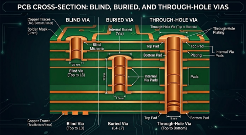
Most fabricators work from a maximum of 1:1 for laser-drilled microvias in UHDI construction. A 75 micron via drilled through a dielectric no thicker than 75 microns or a 50 micron via through a 50 micron dielectric. Push beyond that and plating solution exchange inside the via becomes restricted. Fresh chemistry can't get in. Byproducts can't get out. The result is incomplete plating, thin copper in the via barrel, or voids.
Voids in a standard through-hole via are a reliability concern. In a stacked microvia they're a more immediate problem. Thermal cycling during reflow stresses those voids, and a void inside a copper-filled stacked via creates a failure point that may not show up in electrical test but will show up in the field.
Dielectric thickness and via diameter are both design decisions. Keeping aspect ratio at or below 1:1 isn't a fabricator preference. It's a plating physics constraint the design needs to accommodate and with UHDI there isn’t the margin to push beyond those design rules. And, I know we have all gotten used to pushing those aspect ratios in HDI with subtractive etch!
Stacked Microvias and the Copper Fill Requirement
Most UHDI designs rely on stacked microvias, even though staggered micro vias are often recommended, to achieve the interconnect density the stack-up requires. Stacking is what gives the greatest space savings, but it is also where plating complexity concentrates.
A stacked microvia needs to be copper filled before the next via can be drilled and plated on top of it. The fill has to be complete, flat, and dimensionally consistent. The next laser drill targets the center of that filled via, and if the fill is domed, off-center, or incomplete, the via above it starts with a problem already built in.

Copper fill chemistry is slower and more controlled than standard electrolytic plating, and sensitive to the same geometry variables. Deep, narrow vias fill less reliably than shallow, wider ones. A few things directly affect fill quality: via diameter at or above the fabricator's recommended minimum, consistent dielectric thickness across the full panel, and not stacking more layers than the fabricator's process has been qualified for. Ask about that last one specifically, it is not always a number that makes it into standard DFM feedback.
What Shows Up on First Articles
Plating issues in UHDI don't always show up at the electrical test. A via can pass continuity and still have a plating profile that creates reliability risk. Cross-section analysis is the tool that actually shows what's happening inside the via structure. Treat the first article cross-sections as genuine data collection, not a formality, especially with Ultra HDI designs.
Look for several things: copper thickness consistency in via barrels across multiple samples, not just one location on the panel, the fill profile on stacked vias, a slightly domed or recessed surface tells you something about what the chemistry and geometry are doing to each other, and look at copper thickness variation between dense and sparse areas of the panel.
If any of those show variation that concerns the fabricator, that's the conversation to have in development and well before production. Adjustments at first article are pretty straightforward and expected, but reliability escapes after product ships are not.
Before You Release the Design
A few things to consider:
- Have you calculated the aspect ratio for every microvia and confirmed it's within your fabricator's qualified range?
- Is dielectric thickness in each build-up layer consistent with the via diameter being drilled through it?
- Have you discussed copper fill requirements for stacked vias, including how many stacked layers the fabricator's process is qualified for?
- Has panel copper distribution been addressed, either through copper balancing in the design or a direct conversation about what the fabricator needs?
- The plating process works with the geometry the design provides and getting that geometry right is a controllable variable before releasing to fabrication.
For teams coordinating dense interconnect design, fabrication feedback, and release readiness, Altium Develop helps connect electronics development work across design and manufacturing stakeholders.
Get started with Altium Develop →
Frequently Asked Questions
Why Does UHDI Copper Plating Affect Cost?
UHDI plating can add cost because smaller features often require tighter stack-up control, more process monitoring, additional cross-sections, and closer engineering review between the design team and the PCB fabricator. Stacked copper-filled microvias can also increase fabrication time because each filled level must be completed before the next level is formed.
What Inspection Methods Help Find UHDI Plating Problems?
Cross-section analysis is the primary inspection method for seeing copper thickness, voids, and fill shape inside microvias. Depending on the product risk level, teams may also request coupon testing, thermal stress evaluation, or additional panel-location sampling to compare dense and sparse copper areas.
Which DFM Checks Should Designers Run Before Fabrication?
Designers should review microvia aspect ratio, dielectric thickness, stacked-via count, copper distribution, and the fabricator's minimum qualified feature sizes. Running these checks before output generation helps prevent avoidable DFM holds and keeps the fabrication discussion focused on process capability rather than late layout corrections.

About Author
Related Resources
Related Technical Documentation
Table of Contents
Design to Release, Without the Friction
- Keep reviews tied to the right version
- Reduce handoff confusion and rework
- Spot sourcing and release risk earlier
- Work solo, share when needed
Get Started
Thank you, you are now subscribed to updates.