


Amplified Benefits: Flexible Circuits with Ultra-HDI conductors


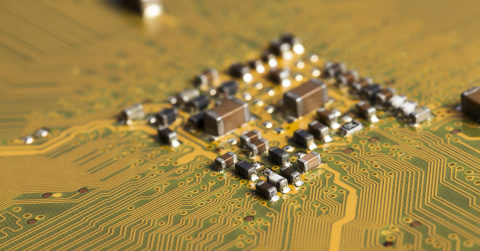
Sometimes 2 + 2 does NOT equal 4, sometimes the combination of two technologies can amplify the benefits of both to something far greater. Today’s blog is going to shine a light on the combination of using both flexible materials and ultra-HDI feature sizes, specifically, trace and space that is less than 50 microns and in fact is now being produced in the United States with 20-micron trace and space using traditional printed circuit board fabrication equipment.
What are the benefits of using flexible circuit construction?
- Solves a packaging issue: Material can be bent and folded around corners, provide 3 axis connection, and has no discrete pieces. Electronic components and functional elements can be placed in the optimal position within the product with the flexible circuit able to be bent, folded, and formed to make the connections. This is where the imagination is taken to task!
- Reducing space and weight needed: Flexible circuits can eliminate bulky wire and solder connections and depending on components and structure, can save up to 60% in weight and space, significantly reducing package size. Flex materials also provide a lower profile than traditional rigid board solutions.
- Biocompatibility: Polyimide materials are an excellent choice for bio-compatibility and are regularly used for that reason in both medical and wearable applications. Advanced technology can also replace copper conductors with gold conductors giving a fully bio-compatible option.
- Reduced assembly costs: Replacing bulky wire and cable reduces or eliminates wiring. This reduces not only the assembly labor costs but the cost of the wire, the cost of generating multiple purchase orders, receiving and inspection, and kitting.
- Facilitates dynamic flexing: Flexible circuits, when properly designed, can withstand millions of flexes. Disk drives are a common example with 10’s – 100’s of millions of flex cycles. Another good example is the hinges on our laptops. These flexes will withstand 10’s thousands of flexes over the life of our computers.
- Thermal management: Polyimide materials are able to withstand high heat applications and thin polyimide dissipates heat much better than thicker, less thermally conductive materials.
What are the benefits of Ultra-HDI?
First, because this is a relatively new term, the definition of Ultra-HDI, per IPC’s recently established working group is a design that includes one or more of the following parameters:
- Line width below 50 microns
- Spacing below 50 microns
- Dielectric thickness below 50 microns
- Micro via diameter below 75 microns
Ultra-HDI is currently being offered by PCB fabricators with circuit trace and space as tight as 20 micron and 12.5 micron is expected to be available later this year.
Even if we don’t push the boundary all the way to 12.5 micron, using a 25-micron trace and space has several benefits:
- Dramatic size and weight reduction over current state-of-the-art.
- Reduced layer count, micro vias and lamination cycles – for greater reliability.
- Tight spacing and impedance control (< 5%) for all line widths, from 15 microns and above
- Aspect ratios greater than 1:1 for metal traces – for improved signal integrity
- RF performance is better than traditional subtractive-etch processes.
- Reduced costs - especially for complex, high-performance boards.
2 + 2 doesn’t ALWAYS equal 4
Looking at even just the first two to three benefits of each technology, one can see the overlapping benefits. Flexible materials help solve a packaging issue and GREATLY reduce size and weight. Ultra-HDI technology has similar benefits. Moving from a 75-micron trace to a 25 micron trace allows the printed circuit board designer to either significantly reduce the overall size of the flexible circuit board or reduce the number of routing layers necessary to make connections.
I don’t think it is any stretch of the imagination to envision the significant benefits to size and weight when incorporating both flexible materials and ultra-HDI feature sizes, replacing traditional rigid materials with circuit trace and space created with subtractive etch technology.
Bonus: If the A-SAP™ process is selected to create the Ultra-HDI features, this process is done by etching away all copper and adding metal back to create the conductor pattern. Polyimide and LCP materials are often selected for Bio-compatibility reasons. The A-SAP™ can create conductor patterns with gold and other noble metals eliminating all copper and nickel from the process creating a unique biocompatible solution.
These ultra-HDI techniques are changing the way PCB designers look at solving complex design issues. If you are interested in learning more about SAP processes, please refer to a few of our previous blogs. We have gone through the basics to SAP processing, recently looked at some of the top questions related to the printed circuit board stack up and explored the design space around the possibility of utilizing these ultra-high density circuit trace widths in the BGA escape regions and wider traces in the routing field. The benefit is a reduction in circuit layers and the concern is maintaining 50-ohm impedance. Eric Bogatin recently published a white paper analyzing just this benefit and concern.
Please reach out with your questions about Ultra-HDI or flexible circuit technology!
About Author
Related Resources
Related Technical Documentation
Table of Contents
Design to Release, Without the Friction
- Keep reviews tied to the right version
- Reduce handoff confusion and rework
- Spot sourcing and release risk earlier
- Work solo, share when needed
Get Started
Thank you, you are now subscribed to updates.

