







Ultra HDI Is Changing What “Assembly-Friendly” Looks Like

At a Glance
Discover how Ultra HDI shifts PCB assembly requirements. Explore stencil design, inspection limits, and rework constraints at fine-pitch BGA layouts.


Most dense board designs, or any board design for that matter, reach a point where they look finished enough that everyone starts to relax. The routing is done with impressive density and a strong escape strategy that didn’t push the full design to the limits. The fabricator has reviewed it, and everything seems ready for production.
But Ultra HDI design for manufacturability in a high mix low volume environment is not yet perfectly understood. Assembly of Ultra HDI also requires a shift in mindset. At Ultra HDI densities, many assembly constraints directly influence footprint selection, routing strategy, and PCB layout decisions long before manufacturing begins. Once solder paste, placement accuracy, inspection, and possible rework enter the picture, some of the assumptions that worked fine in conventional PCB design are no longer applicable.
A lot of the UHDI discussion has centered on fabrication capability, which makes sense. Can the features be etched cleanly? Can the microvias be drilled and plated reliably? Can registration be held tightly enough to support what the layout is asking for? Those are valid concerns.
Ultra HDI technology changes more than PCB fabrication. It also reshapes PCB assembly, inspection, and long-term reliability. As component pitch decreases below 0.35 mm, stencil design, soldermask strategy, placement accuracy, inspection capability, and rework planning become design decisions rather than manufacturing considerations. Successful Ultra HDI projects require close coordination between PCB designers, fabricators, assemblers, and manufacturing engineers from the earliest stages of layout development.
Key Takeaways
- At UHDI pitch below 0.35 mm, stencil aperture area ratios drop below reliable thresholds, requiring thinner stencils or type 5+ paste – decisions that must be made before layout begins.
- Soldermask dam stability fails below 75 µm with standard LPI materials, forcing a choice between dry-film soldermask or mask-defined pads that directly affects routing and escape strategy.
- Placement, paste registration, and board registration tolerances stack at UHDI pitch, consuming 25-40% of available pad geometry and compressing the margin against bridging and joint failure.
- AOI confidence degrades below 0.3 mm pitch due to shadowing and reduced fillet size, meaning X-ray inspection requirements must be planned into the test and cost model from the start.
Paste Transfer and Stencil Aperture Geometry
Solder paste transfer efficiency is governed by the area ratio of the stencil aperture, defined as the open area divided by the sidewall area. For conventional SMD pads, maintaining an area ratio above 0.66 is standard and generally sufficient for reliable paste release. At UHDI pad sizes (especially for 0.3 mm pitch BGAs and below), aperture dimensions shrink to the point where achieving this ratio with standard stencil thicknesses becomes impossible. For Ultra HDI designs, stencil development should be considered part of the PCB design process rather than a downstream manufacturing activity.
For example, a 0.2 mm round aperture in a 100 µm stencil yields an area ratio of only 0.50, well below the threshold for reliable paste release. Reducing stencil thickness to 75 µm or 60 µm can recover some margin, but this introduces secondary problems: reduced paste volume on larger pads elsewhere on the board, and increased sensitivity to stencil flatness and gasketing. Step stencils can partially address this, but add cost and introduce transition zones with unpredictable paste volume. These tradeoffs demonstrate why PCB designers and assembly engineers should review stencil strategy together before footprint libraries are finalized.
The implication is that pad geometry and stencil design are tightly coupled decisions at UHDI pitch. Selecting a BGA package with 0.25 mm pitch commits the assembly process to a specific stencil technology and paste type before layout even begins. Footprint libraries built for conventional HDI often assume standard stencil thickness, and these assumptions fail silently when pitch drops below 0.35 mm.
Soldermask Dam Stability at Fine Pitch
Soldermask between pads prevents solder bridging and controls paste registration. At conventional pitch, liquid photoimageable (LPI) mask with dam widths of 75 µm or greater is process-stable. Below 75 µm, LPI dams become unreliable due to exposure and development tolerances, adhesion limits, and mechanical fragility. Soldermask strategy affects both manufacturability and long-term assembly yield, making it an important consideration during footprint development rather than fabrication review alone.
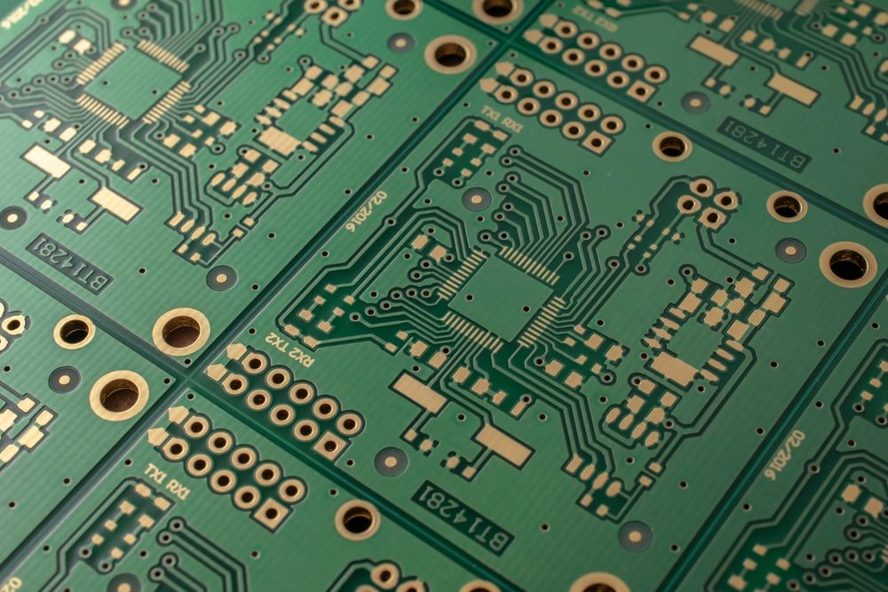
Dry-film soldermask can extend the practical limit to approximately 50 µm dam widths, but requires different processing equipment and introduces its own constraints, such as conformality over surface topography. Below 50 µm, mask dams become a yield risk regardless of material, and many assemblers will request mask-defined pads or solder-dam-free designs in dense regions.
The choice between mask-defined and non-mask-defined (NSMD) pads at fine pitch is not just a soldering preference. It affects copper exposure tolerance, pad-to-trace clearance, and the inspection reference for joint evaluation. Designers working at 0.3 mm pitch and below must confirm the assembler's mask capability before finalizing pad definitions, as changing from NSMD to mask-defined after layout completion typically forces re-routing of the escape pattern.
Regions where soldermask stability is most critical:
- Fine-pitch BGA footprints below 0.35 mm pitch, where dam widths drop below 75 µm
- Dense passive clusters with 0201 or 01005 components, where mask registration affects paste containment
- Compact RF sections where mask thickness variation affects impedance of nearby traces
Placement Tolerance Stacking in Dense Geometry
Pick-and-place machine accuracy is typically specified as ±25 µm to ±50 µm at 3-sigma, depending on the machine and vision system. At conventional pitch, this tolerance is a small fraction of the pad dimension and does not meaningfully affect joint formation. At UHDI pitch, placement tolerance consumes a significant percentage of the available pad area. Unlike conventional PCB designs, Ultra HDI layouts leave very little tolerance for cumulative manufacturing variation, making tolerance analysis an essential part of design validation.
For a 0.25 mm pitch BGA with 0.12 mm pads, a ±35 µm placement offset represents nearly 30% of the pad radius. The joint may still form, but the self-centering force during reflow is reduced, and the margin against bridging to adjacent pads is compressed. When placement tolerance is combined with paste registration tolerance (typically ±20 µm to ±30 µm from stencil printing) and board registration tolerance (±25 µm from panel fiducials), the total stacking can approach or exceed the available clearance between adjacent pads.
Assembly Factor | Conventional HDI (≥0.4 mm pitch) | UHDI (<0.35 mm pitch) |
Paste transfer | Area ratio >0.66, 100–125 µm stencil | Area ratio <0.60, requires thinner stencil or type 5+ paste |
Soldermask dams | LPI at 75+ µm, process-stable | LPI marginal below 75 µm; dry-film required below 60 µm |
Placement tolerance | Machine accuracy is a small fraction of pad | Tolerance stacking consumes 25–40% of pad geometry |
Inspection access | Standard AOI lighting and angles adequate | Shadowing, reduced contrast on small joints |
Rework feasibility | Localized thermal event, adjacent joints unaffected | Thermal coupling to neighbors, risk of collateral reflow |
Instead of specifying tighter placement tolerances, note that the pad geometry, mask opening, and paste volume must together provide enough self-centering margin to tolerate the expected placement distribution. This requires simulating or calculating the worst-case overlap condition and confirming that joint formation remains reliable at the 3-sigma placement offset.
Inspection Access and Confidence at Fine Pitch
Automated optical inspection (AOI) relies on contrast between solder, pad, and mask surfaces, combined with angular lighting to reveal joint shape. At conventional pitch, the joint fillet is visible from multiple angles, and the spacing between components allows adequate illumination. Below 0.3 mm pitch, several factors degrade inspection confidence:
- Component body height relative to pitch creates shadowing that obscures joints from certain camera angles.
- Reduced joint volume at fine pitch produces smaller fillets with less reflective surface area.
- Dense placement of adjacent components further restricts lighting angles.
The result is that AOI may report a pass on joints that are actually marginal, or flag false failures on joints that are acceptable but poorly illuminated.
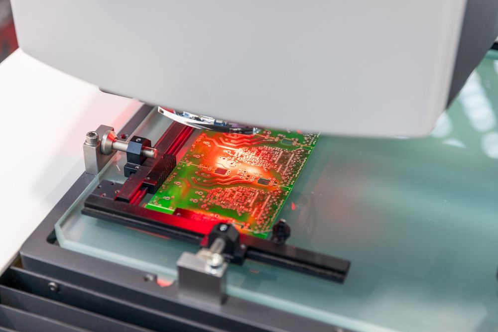
X-ray inspection can address some of these limitations for BGA joints, but adds cycle time and cost. More importantly, X-ray interpretation at fine pitch requires careful void-percentage criteria and consistent imaging parameters. A design that relies on X-ray for first-article validation should account for this in the test plan and cost model from the beginning, not as a reactive measure after AOI proves insufficient.
Rework and Repair Constraints
At UHDI pitch, rework feasibility is significantly reduced. Localized thermal events during rework can easily affect adjacent joints due to the proximity of pads and the reduced thermal mass of fine-pitch components. The risk of collateral reflow or damage to neighboring joints increases, making traditional rework approaches less reliable. This must be considered in both the design for assembly and the long-term serviceability plan.
- Engage with assembly partners early: Confirm stencil, mask, and placement capabilities before finalizing pad and footprint libraries.
- Simulate worst-case tolerance stacking: Ensure that pad geometry and paste volume provide sufficient margin for reliable joint formation at the expected placement and registration tolerances.
- Document inspection requirements: Specify AOI and X-ray inspection needs in the assembly documentation, including keep-out zones and fiducial placement.
- Plan for rework limitations: Recognize that rework at UHDI pitch is riskier and may require specialized equipment or acceptance of higher scrap rates.
Any review of a UHDI layout should occur at placement-complete, before detailed routing begins. Changing pad definitions, mask strategy, or component spacing after routing is complete typically forces a full re-route of the affected region, which at UHDI density may propagate changes across multiple layers. Early coordination with both the fabricator and assembler eliminates the most common sources of assembly-driven redesign and ensures that the layout reflects achievable process capability rather than theoretical design rules.
The biggest risks in Ultra HDI assembly are coordination failures as much as design failures. Altium Agile Teams connects electrical engineers, mechanical engineers, and procurement in one platform, so the decisions that determine assembly yield are visible to everyone who needs to act on them.
Learn more about Altium Agile Teams →
Frequently Asked Questions
What stencil thickness should I use for Ultra HDI assembly?
Standard 100 µm stencils cannot achieve the area ratio needed for reliable paste release at UHDI pitch. For pads below 0.35 mm pitch, stencil thickness should be reduced to 75 µm or 60 µm, or step stencils used to manage the difference between fine-pitch and standard pads on the same board. The stencil strategy must be determined before layout is finalized, not after.
When should I use mask-defined pads instead of NSMD pads at fine pitch?
Below 75 µm soldermask dam widths, standard LPI mask becomes unreliable. When dam widths drop to this level, typically at 0.3 mm pitch and below, mask-defined pads or dry-film soldermask are required. The choice affects copper exposure, pad-to-trace clearance, and escape routing, so it must be confirmed with the assembler before pad definitions are locked.
Can AOI reliably inspect Ultra HDI solder joints?
AOI confidence degrades below 0.3 mm pitch. Component shadowing, reduced fillet size, and restricted lighting angles mean AOI can pass marginal joints or fail acceptable ones. X-ray inspection is needed for BGA joints at UHDI pitch, but requires defined void-percentage criteria and consistent imaging parameters planned into the test strategy from the start.
Is rework feasible on Ultra HDI boards?
Rework at UHDI pitch carries significantly higher risk than on conventional boards. The reduced thermal mass of fine-pitch components and tight pad spacing means localized rework heat easily affects adjacent joints. Teams should plan for rework limitations during design, including potential acceptance of higher scrap rates or the need for specialized equipment, rather than treating it as a routine corrective option.

About Author
Related Resources
Related Technical Documentation
Table of Contents
Speed at Scale. Structured Repeatability. Secure Flexibility.
- Start up fast with out‑of‑the‑box workflows
- Collaborate using ECAD‑MCAD codesign tools
- Manage BOMs with live supply chain part data
- Manage access and security as teams scale
Contact Us
Thank you, you are now subscribed to updates.