


Avoid Costly Interconnect Errors: Essential Multiboard PCB Layout Strategies for Reliable Designs

At a Glance
Avoid costly multiboard PCB interconnect failures by designing better connector pinouts, launches, return paths, and mechanical fits before layout release.


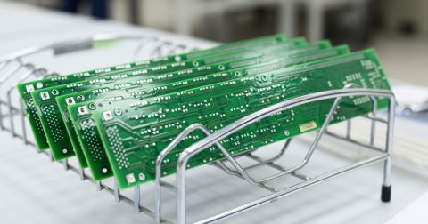
Stacked PCBs, mezzanine connectors, flex, and harnesses force multiple interfaces into a small volume, usually with vibration, temperature cycling, and conducted and radiated EMI. In that environment, many field and bring-up failures originate at the interconnect, not inside a single board. Typical root causes are pin assignments that ignore return current paths, inconsistent net naming between schematic and harness, connector transitions that add discontinuities, and mechanical assumptions that were never validated against the actual stack height and tolerances.
The strategies in this article show how to avoid costly interconnect errors through connector pinout design, signal and power integrity at connector transitions, mechanical fit, and shift-left verification.
Key Takeaways
- Start with system-level interconnect intent so layout decisions stay aligned with what actually needs to connect.
- Design pinouts, return paths, and transitions for SI, PI, and EMI continuity across every boundary.
- Use a shared product environment to keep changes synchronized across boards, harnesses, and BOM decisions.
Where Multiboard Interconnects Go Wrong
Interconnect failures in multiboard systems usually do not begin as mysterious subsystem problems. They begin at a connector boundary, in a flex transition, or in a harness segment where the electrical definition, mechanical definition, and documentation stopped matching. The symptom might be an intermittent reset, an unstable high speed channel, excess heating in a power path, or a board that works on the bench and fails once installed in the enclosure. The mistake is treating the interconnect as a secondary implementation detail instead of part of the board design itself.
For PCB designers, the relevant question is not whether two boards connect. The real question is whether the transition between them preserves the required electrical behavior, fits the mechanical constraints, and remains buildable and testable across revisions. That requires more than net continuity. It requires correct pin assignment, controlled launches, continuous return paths, current capacity, shield and ground strategy, flex or harness implementation rules, and documentation that fabrication, assembly, and test can all use without reinterpretation.
Logical Connectivity Errors
Some of the most expensive interconnect problems are still basic definition errors. Swapped nets, missing reference pins, inverted differential polarity, inconsistent connector numbering, and mismatched orientation callouts can survive longer than they should when teams assume the connector table is correct and nobody rechecks the physical implementation. These are not difficult problems. They persist because schematic symbols, footprints, mechanical orientation, and interconnect documentation are often created or revised separately.
A multiboard design needs one interconnect definition that maps directly into the schematic, connector pinout, PCB footprint orientation, harness drawing, and test documentation. If connector numbering changes between views, or if mating orientation is assumed instead of shown explicitly, the result is no longer a documentation problem. It becomes a board spin, a harness rework, or a bring-up delay.
Typical definition errors include:
- Pin numbering mirrored or rotated between mating parts
- Differential pair polarity reversed at one connector
- Power and return pins separated physically even though the schematic is correct
- Orientation notes shown in MCAD or a drawing, but not in the PCB documentation set

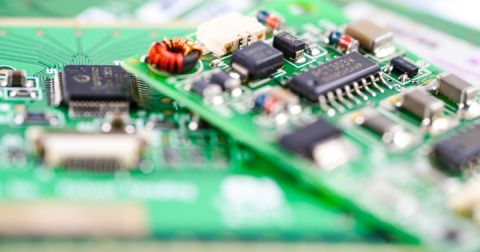
Connector Pin Assignment
Connector pin assignment should be treated with the same care as stackup design or component placement. A good pinout reduces routing difficulty, keeps return paths short, limits coupling between unlike nets, and makes the electrical intent obvious during review. A poor pinout forces detours, breaks return path continuity, mixes noisy and sensitive nets, and pushes avoidable problems into layout and test.
Signals need to be grouped by electrical behavior, not just by function. Differential pairs need paired assignments that remain adjacent through the launch and mating interface. High edge rate signals need nearby return references. High current power pins need enough parallel conductors and return capacity to control heating and voltage drop. Sensitive analog signals should not share a local pin field with fast digital edges or noisy power conversion nodes unless that decision is deliberate and justified.
| Interconnect type | What needs to be checked | Typical result when ignored |
| Differential pairs | Pair adjacency, polarity, nearby returns, breakout symmetry | Common-mode conversion, skew, launch discontinuity |
| High current power | Parallel contacts, return sharing, contact loading, voltage drop | Heating, droop, overstressed contacts |
| Sensitive analog | Separation from high dv/dt or high di/dt nets, return strategy | Injected noise, unstable measurements |
| Shielded I/O | Shield termination location and bonding method | EMI leakage, unintended shield current |
Connector Launches and Return Path Continuity
A board-to-board or board-to-cable transition is not electrically transparent. The connector footprint, breakout routing, via field, plane changes, and mating structure all contribute discontinuity. If the article mentions impedance control at the boundary, it needs to say what that means in practice: the launch geometry has to be designed as part of the interconnect, not treated as ordinary fanout routing. That means checking pad dimensions, antipads, via transitions, stub length, ground reference placement, and the path available to return current as the signal crosses the connector region.
The phrase "reference continuity" could refer to multiple problems. Usually that problem is a broken return path, excess loop inductance, or common-mode conversion created when the signal changes reference (or has no reference) at the connector. In practice, that means ground pins must be assigned where they support the signal field, stitching vias must connect reference regions where needed, and plane interruptions near the launch should be treated as a design error unless there is a clear reason and a validated mitigation.
The most useful launch checks are usually these:
- Padstack and antipad geometry through the breakout
- Stub length and number of layer transitions
- Ground pin placement relative to high speed signals
- Plane voids, split crossings, or missing stitching vias near the launch
Power Transfer Across Interconnects
Power distribution across a connector is one of the easiest places for a design to look correct in the schematic and fail in hardware. The connector and off-board conductors add resistance and inductance, so transient current demand can produce droop, heating, sequencing instability, or nuisance resets even when the nominal current rating looks acceptable on paper. Connector current ratings also depend on contact count, temperature rise, conductor size, airflow, and loading pattern, so choosing a part by its headline rating alone is not enough.
Power pins need to be assigned as current paths, not just as labeled nets. Parallel contacts, nearby returns, conductor size, and entry-point decoupling all affect whether the receiving board sees a stable supply during dynamic load events. If shield and chassis connections are involved, those terminations also need to be defined intentionally. A vague grounding scheme at a cable entry or board boundary is usually just a delayed EMI problem.
Mechanical Fit, Flex Regions, and Harness Constraints
Interconnect errors are often created by mechanical assumptions that never made it back into the PCB. Connector placement has to be checked against insertion path, mating clearance, board spacing, tolerance stack-up, retention hardware, and service access. Blind-mate systems are especially unforgiving because the connector is part of a tolerance system, not just an electrical interface. If the placement only works in nominal CAD alignment, it is not robust.
The same point applies to flex and harness segments. Bend radius, repeated flexing, stiffener location, copper distribution, strain relief, and wire exit direction are board implementation issues, not secondary packaging details. If a flex region includes vias, heavy copper concentration, or badly placed transitions near an active bend area, the reliability problem is already in the design. If a harness exits a connector in a way that violates bend constraints or creates installation stress, the problem is already in the layout.

Verification Before Layout Release
Interconnect verification needs to happen before the layout is effectively frozen. It requires specific engineering checks while the pinout, placement, connector selection, and boundary definition can still be changed without major rework. At minimum, that includes continuity checks across mating interfaces, explicit review of connector orientation and numbering, current-path review for power contacts, creepage and clearance checks where relevant, and SI or PI analysis on the boundaries that actually set margin.
For mechanically constrained designs, it also means checking the assembled geometry, not just the individual board. Connector keepouts, insertion path, harness clearances, strain relief space, and board-to-board spacing should all be confirmed in assembly context. The documentation also needs to stay synchronized so that a connector revision updates the related drawings, harness definition, and test requirements instead of creating another round of mismatched files.
A practical pre-release review should answer these questions:
- Does the pinout support the required routing, return paths, and current paths?
- Does the launch preserve the intended electrical behavior across the transition?
- Do the PCB, drawings, and mating assumptions agree everywhere?
- Are the flex or harness constraints reflected in the board implementation?
Interconnect problems are rarely caused by a lack of general best practices. They are caused by specific design decisions that were left ambiguous until they became expensive to change. The article needs to stay centered on those decisions: pin assignment, launch design, return path continuity, current transfer, mechanical fit, flex and harness constraints, and the documentation needed to build and verify the assembly correctly.
The most expensive interconnect failures are the ones that surface as intermittent resets and failed first articles, long after the boundary decisions that created them. The teams that catch these issues earlier do so by keeping interconnect intent clear, reviewable, and tied to the active design as it evolves. That’s the kind of design‑time discipline Altium Develop is built to support. Try Altium Develop today!
Frequently Asked Questions
Why do multiboard PCB systems fail at the interconnect instead of on the board?
In stacked, flex, or harnessed systems, the interconnect is where electrical, mechanical, and documentation assumptions collide. Many failures originate from broken return paths, poor connector launches, mismatched pinouts, or mechanical tolerances that were never validated at the system level. These issues often pass schematic review but surface later as intermittent resets, EMI problems, or bring‑up failures.
What are the most common connector and pinout mistakes in multiboard designs?
Common mistakes include incorrect pin numbering between mating parts, reversed differential polarity, separating signals from their return paths, and grouping noisy and sensitive nets together. These errors persist when schematic symbols, footprints, harness definitions, and mechanical orientation are not derived from a single interconnect definition. Once implemented, they are costly to fix and often require a board respin or harness rework.
How should connector launches and return paths be designed for signal and power integrity?
Connector launches must be treated as controlled transitions, not simple fanouts. Pad geometry, antipads, vias, reference planes, and nearby ground pins all determine whether impedance and return current continuity are preserved across the interface. Ignoring these details leads to discontinuities, common‑mode conversion, power droop, and EMI issues.
When should interconnects be verified in a multiboard PCB project?
Interconnects should be verified before layout release, while pinouts, placement, and connector choices can still be changed. This includes reviewing electrical behavior across connectors, power current paths, mechanical fit, flex or harness constraints, and documentation consistency. Early verification prevents late‑stage failures that are expensive to diagnose and fix.

About Author
Related Resources
Related Technical Documentation
Table of Contents
- Key Takeaways
- Where Multiboard Interconnects Go Wrong
- Logical Connectivity Errors
- Connector Pin Assignment
- Connector Launches and Return Path Continuity
- Power Transfer Across Interconnects
- Mechanical Fit, Flex Regions, and Harness Constraints
- Verification Before Layout Release
- Frequently Asked Questions
- Why do multiboard PCB systems fail at the interconnect instead of on the board?
- What are the most common connector and pinout mistakes in multiboard designs?
- How should connector launches and return paths be designed for signal and power integrity?
- When should interconnects be verified in a multiboard PCB project?
Design to Release, Without the Friction
- Keep reviews tied to the right version
- Reduce handoff confusion and rework
- Spot sourcing and release risk earlier
- Work solo, share when needed
Get Started
Thank you, you are now subscribed to updates.