What's With All the Layers in PCB Footprints?
Every PCB needs components, even if those components are marked DNI and never make it into the final assembly. Each component has a PCB footprint, and each PCB footprint has information on various layers. The layers in a PCB footprint represent important information about the real component, but not all of them are defined by the user.
Because we have recently received a few viewer questions on the Altium Academy channel about PCB footprints and the essential layers they should contain, this article will focus on what information is contained in each footprint. From this information, you should be able to see which footprint layers are most essential and what information they should contain.
Important Layers in PCB Footprints
If you’re a new PCB design software user, and you’re taking time to create your first custom footprint, you’ll notice many layers in your footprint editor. These layers match the basic layers that are used to create your PCB layout, but the layers in your footprint need to include specific information. Some of this information must be created manually when building the component footprint, and some information is auto-generated in the PCB editor.
The table below outlines the complete list of layers needed to create a footprint. The layer names with an asterisk (*) are required to create a minimum functional footprint, although additional information will be needed to create a PCB footprint.
|
|
|
|
|
|
|
|
|
|
|
|
|
|
|
|
|
|
|
|
|
|
|
|
|
|
|
|
|
|
|
|
|
|
|
As you can see, most of the layers in a PCB footprint need to be created manually, but most of the absolutely required layers are auto-generated. So of course, this begs the question, which of the manual layers should you create, despite the fact that not all of these are required for usage in a PCB layout?
When you see “auto-generated” in this table, it means that the layers are generated by the PCB design rules engine, and you are not required or unable to create this information manually in your PCB footprints. In Altium, these are managed inside the PCB layout in the PCB Rules and Constraints Editor.
Keepouts
Another example that is quite important both for fabrication, assembly, and EMI/EMC is keepouts. A keepout layer is used to ensure that everything else in the PCB layout is kept away from that part of the PCB footprint, including everything from copper to other components in the PCB layout. Most components will not need a keepout layer.
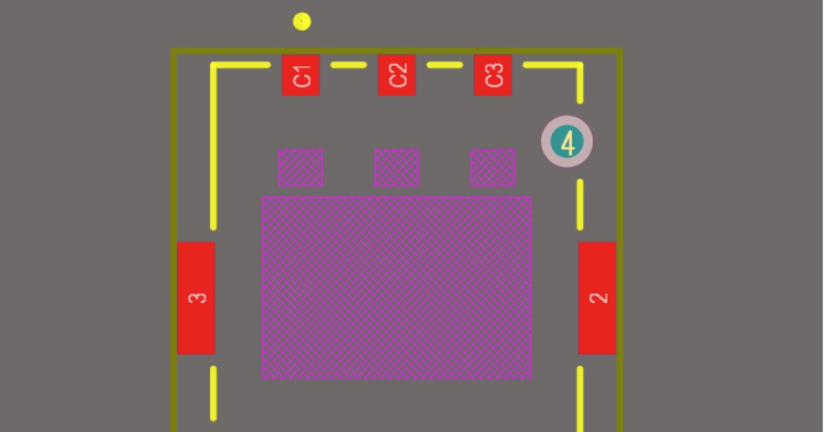
An example of a keepout layer on a PCB component is shown below. The point of this layer is to prevent placement of components and routing in the keepout area. Because this component is a connector, but the type of component may not be obvious by just looking at the footprint, it makes sense to define placement and routing limitations using keepouts.

Courtyards
A courtyard layer is used to draw the required clearance around a PCB footprint as specified in the IPC-7351 standard. The standard gives a courtyard clearance recommendation based on three density levels:
- Most (lowest density):
- Surface Mount Components: Minimum 0.25 mm (0.01 inches) courtyard clearance.
- Through-Hole Components: Minimum 0.5 mm (0.02 inches) courtyard clearance.
- Nominal (moderate density):
- Surface Mount Components: Minimum 0.15 mm (0.006 inches) courtyard clearance.
- Through-Hole Components: Minimum 0.25 mm (0.01 inches) courtyard clearance.
- Least (highest density):
- Surface Mount Components: Minimum 0.1 mm (0.004 inches) courtyard clearance.
- Through-Hole Components: Minimum 0.15 mm (0.006 inches) courtyard clearance.
An example courtyard outline showing the allowance for courtyard excess is shown below:

This outline is purely a tool used by the PCB designer to ensure they do not cluster components too close together. Obviously, it should be clear that different acceptable density levels will require different courtyard drawings, and you may find that a courtyard has been ignored in a component while instead a clearance outline is placed in the silkscreen layer to identify clearance limits. Unfortunately, this might lead to guesswork during layout, and it could possibly require some component shifts before a board can pass into an SMT line if the silkscreen markings do not indicate insufficient clearance.
3D Body
CAD systems that support 3D viewing of the PCB will also allow you to assign a 3D model to a component. This can be assigned as a STEP model or as another solid model format. In the component footprint, the 3D model layer shows the extents of the 3D model projected into a 2D plane from an overhead view (this is the purple area above). The details of the package can only be seen in a 3D view, they will not be visible in the corresponding layer in the PCB footprint.

Assembly Outlines
The assembly outline for a component is only needed to generate an assembly drawing, which your assembler can use for verification that components are being placed in the correct locations. Your fabrication house does not need assembly layers exported as Gerbers. Your assembler might use these internally to create their own assembly drawings, or you can use these outlines to create your own assembly drawings, either in a drafting tool or in the Draftsman tool in Altium.
What’s unique about Draftsman in Altium is that the top surface of the 3D body can also be projected into an assembly drawing, as shown in the example below. Normally, if you wanted to create this much detail in a drafting application, you would need to manually project all of your 3D body models into DXF files, and then compile those DXF files into a single layer in an assembly drawing. Draftsman does this for you and instantly generates highly detailed drawings like the example shown below.

Whenever you need to create custom footprints or access pre-made footprints that are validated by manufacturers, make sure you use the complete set of industry-leading PCB design tools in Altium. To implement collaboration in today’s cross-disciplinary environment, innovative companies are using Altium to easily share design data and put projects into manufacturing.

