


Advanced High Density PCB Layout and Design in Altium

At a Glance
HDI design and high density interconnect routing require implementing a specific process in the PCB stackup and design rules. Learn more in this chapter of Happy Holden's guidebook.


HDI PCB design and manufacturing push electronics and circuit boards to their limits. As electronics become faster and more capable, they require greater functionality in a smaller package. From smartwatches to data centers, HDI design is slowly becoming the norm rather than the exception. Keeping up with new technology and design techniques means that designers need to rethink how they layout components, as well as design interconnects and vias in their boards.
Modern electronics carry more components and functionality than ever before, and designers need to understand many of the finer points of HDI PCB design. It starts from a simple idea: reduce the size of traces, vias, component, and pads in order to fit more components into a smaller area. However, this requires changing the manufacturing process, and any HDI PCB needs to be manufacturable at scale. Here’s how you can be successful when designing your next HDI PCB and how you can prepare for circuit board manufacturing with HDI PCB processes.
HDI PCB Stackup Design
Implementing HDI design techniques on your board requires designing the right stackup; this is the first step in starting a PCB layout for an HDI PCB. You’ll need to ensure that you can route the high density of signals you need between components while ensuring signal integrity and conforming to your manufacturer's DFM constraints.
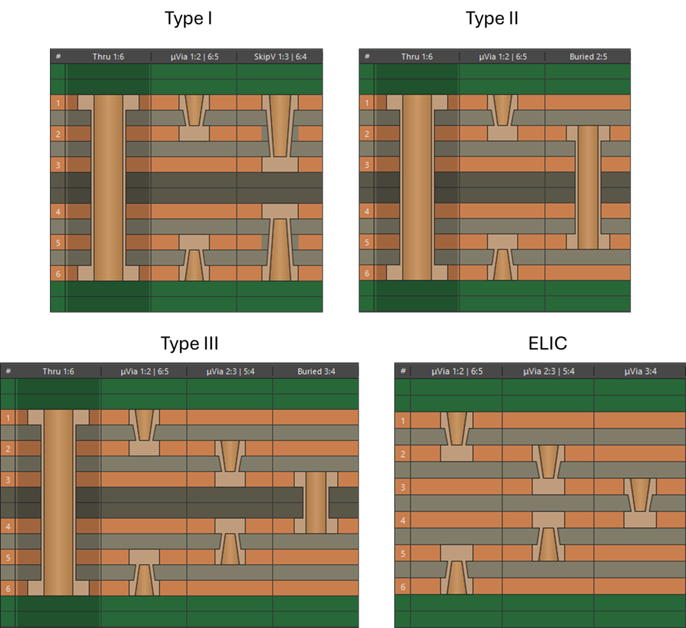
Select a Standardized HDI Stackup
Standard HDI stackups prescribe approaches to selecting layer transitions with microvias which can then be put through a sequential lamination process to build the HDI stackup. The four common types of HDI PCB stackup are shown below.
The first three types of stackup use a buried core via as a central sub-lamination, and the build-up film layers are laminated around this sub-lamination. The ELIC type of HDI PCB stackup uses build-up films through the entire stackup, allowing for blind/buried microvias throughout the design. In today's HDI designs, the most commonly used type of stackup is Type III. Once the stackup type is chosen, the number of build-up films and via sizing need to be determined.
Determine Build-up Layer Requirement
The most common approach to determine the number of build-up layers required in the design is to count up the number of signal layers required for escape routing from the largest BGA in the PCB. The image below shows two BGAs with 0.5 mm pin pitch. With this pin pitch value, we would not be able to fit mechanically-drilled vias in a dog bone fanout arrangement. Placing these in-pad would require a large number of sub-laminations from the top layer, which will result in heavy copper from multiple plating cycles and thus excessively large clearance and etch limits.
Due to these factors, the design is forced to be an HDI design as it will require fewer laminations and the etching feature size/clearance limits can remain small (2-3 mil typically). From the image below, we can count up that the smaller BGA requires 3 signal layers when microvias are used, and the larger BGA requires 5 signal layers.

Two BGAs shown in a PCB layout in Altium.
Based on these signal layer counts, and depending on the other layers expected in the design, one might expect to use 3 build-up layers on each side in the design. These may need to be stacked or staggered, depending on the fabrication capabilities and material used for the build-up film. Once the number of required build-up layers is determined or if a standard HDI stackup will be used, the designer can implement the microvia structures listed below.
Defining Microvia Structures
HDI boards require the use of microvias for layer transitions. Microvias are simply small vias that require a specialty manufacturing process (i.e., other than mechanical drilling). These structures are defined by the IPC-2226 HDI Design Standard. The various microvia structures you can access in Altium are shown below, which includes staggered, skip, and buried types of microvias.

HDI PCB via definition in Altium’s layer stack manager.
Please note the following: Always check with your fabrication house before starting any HDI design to ensure your stackup and your preferred via arrangement can be fabricated.
For now, take a look at the types of vias used in HDI PCB stackups to determine the right mix of vias for your application. Then use this information to construct a stackup for your design.
Staggered Blind/Buried Vias
Staggered microvias on a single side or both sides with buried through-hole vias between inner layers is the most common and lowest cost HDI PCB layer stackup. When using multiple microvias to connect inner layers, it is preferred the microvias be offset by some angle and the vias not be stacked (e.g., as in a crankshaft). This will minimize any thermal excursions if the vias heat up to high temperatures. Be sure to contact your circuit board fabricator for material and process compatibility if you plan to produce an HDI PCB at high volume.

Build-up of multiple HDI PCB layers connected with buried vias.
Skip Blind Vias
A skip microvia is special in that it is used to ‘skip’ the next adjacent layer, as seen in Figure 7. Because a skip microvia can be the deepest of microvias, it is important that the designer be aware of a fabricator’s capability to produce and metallize such a microvia. Many circuit board manufacturers will not have this capability and will give your board no-bid status if they spot this in your Gerber files. With all blind vias, the aspect ratio may be reduced to 0.7:1 or even 0.65:1, so that the surface pad and target pad will be larger than the via length. The via is quite susceptible to fracture at its neck when light copper foil is used to place these vias.

A skip microvia can be used to skip a layer in a multilayer circuit board.
Stacked vias
Stacked microvias use the least amount of board real-estate but are significantly more difficult to fabricate. This stems from the need for the target land of the top microvia having a solid metal surface to connect to. The process requires filling of the microvia either with conductive materials and plating it over (VIPPO) or with the use of “super-fill copper plating” capable of solid copper plating the microvia interior (see the image below).

Stacked microvias require a solid metal surface for the ‘landing pad’ on top of the microvia. The lower portion of the microvia is produced with a laser, and the void is filled and plated over.
Currently, it is recommended that stacked microvias not be stacked on top of a mechanically-drilled buried via. Reliability concerns have arisen from this practice. Be sure to contact your PCB fabricator about this construction and read the IPC White Paper on Performance-Based Printed Board OEM Acceptance-Via Chain Continuity Reflow Test: The Hidden Reliability Threat-IPC-WP-023 (May 2018).
BGA Breakout in HDI Boards
Fine-pitch BGA fanouts are routed either using microvia-in-pad or by using a microvia that is only touching the SMT pad. Note that, for 0.5 and 0.4 mm pitches, the via holes are not required to be in the center of the lands as long as the vias drill diameter and pad diameter are small enough. This is to increase spacing between traces on the inner layers beyond a minimum of 0.05 or 0.075 mm (2 mil or 3 mil respectively), which are typical limits stated by many fabrication houses under an advanced etching process.
In addition to the traditional N-S-E-W dogbone breakout of BGAs, microvias facilitate new BGA breakout methods that greatly increase routing density and lower layer counts. Two of these methods are channels and swing-via placement. In cases where the hole/pad sizes need to be larger, via-in-pad may be required for fine-pitch BGAs. Be sure to contact your PCB fabricator to determine which geometries and via stacking arrangements they can support.
Channels
When a BGA’s total number of signal escapes begin to exceed 400 pins, microvias should generally be used for breakout as rows that cross the BGA, rather than on the peripheral. These form ‘channels’ on the inner-layers and far side of the circuit board. These channels allow access to internal signals in the BGA, thus fewer layers are required for total breakout.
The BGA in Figure 11 is an 1153 pin (34x34) BGA (1.0 mm pitch) and with 132 possible routes per layer (1 trace between vias) plus 20 traces in the channel (5 traces). This means that 8 layers would be required (plus 5 separating plane layers) to connect this BGA to the rest of the circuit board.
If we create more routing channels, we connect more traces per layer and reduce the total number of layers. Channel routing uses blind microvias to form up to 4 additional cross-shaped, L-shaped, or diagonal channels in a BGA fanout. These new channels allow up to 48 extra connections per layer (8x6 traces). Two routing layers and two plane layers can be eliminated.

Routing channels formed by microvias to ease breakout from large BGAs. Channels can be cross-shaped, L-shaped, or diagonal.
Swing Break-Outs for Boulevards
A swing via is actually a pair of vias that are fanned out between two BGA pads to maximize the available area for routing conductors between them. Instead of placing a single breakout via in a standard N-S-E-W dog bone fanout, smaller microvias are used to give enough room for two adjacent breakout vias, as shown in Figure 13. The microvia pads are so much smaller than a through-hole pad that there is room for a surface ground flood down to a 0.65 mm pitch.

Example of swing breakout for a large 0.8 mm pitch BGA that includes surface ground fill.
Via-in-Pad in Fine-Pitch BGAs
In fine-pitch BGAs, such as 0.5 mm or smaller, it is possible that the design does not allow mechanically drilled vias due to the required drill and pad size (e.g., as required for Class 2 or Class 3 compliance) and the clearance requirements that arise with mechanically drilled blind/buried vias. In this case, laser-drilled microvias will need to be placed in the component pads for fine-pitch BGAs. The same can happen with fine-pitch QFNs, although this has become less common due to the diversity of features on BGAs.
These vias are often stacked, as shown in the project example below. These vias need to have low aspect ratio and should be fabricated on a proper build-up film with low CTE value, such as ABF or newer resin-coated copper.

Stacked microvias on a 0.35 mm pitch BGA. This BGA can be routed using two stacked microvias spanning Layers 1-3.
The number of stacking layers will be limited based on the build-up film material being used, total number of build-up layers, and product-specific qualification. Via-in-pad usage may further limit the number of allowed stacked microvias due to the thermal excursions experienced during soldering. For example, in mil-aero designs, the number of stacked microvias in a design with FR4 materials may be intentionally limited due to the thermal expansion of FR4 materials.
Design Rules For HDI PCBs in Altium
Before setting up your PCB design rules in your CAD software, you should always gather your fabricator’s HDI capabilities and use these to define your constraints. The list below is not exhaustive for all possible designs, but it does address most of the fabrication and assembly constraints that would commonly lead to redesigns in an HDI PCB.
- Fabrication constraints:
- Trace width and spacing
- Microvia drill diameter/pad diameter
- Drill-to-drill spacing
- Maximum number of stackup microvias (material dependent)
- Maximum number of build-up layers (material dependent)
- Aspect ratio limits as function of drill diameter/depth
- Available build-up layer materials
- Via fill/cap options
- Surface finish options
- Assembly constraints:
- Part-to-part spacing
- IPC density level support
- Available solder paste material
- Available solder paste type
- Recommended thermal relief placement on SMD pads
- Recommended venting via placement where applicable
For fabrication, two of the most important rules to apply in the PCB layout are microvia sizing, copper clearances, and trace width/clearance limits in the design. These can be easily applied in Altium on a Net Class basis or inside specific regions of the PCB. The examples below show how these can be easily applied in an HDI PCB layout.
Microvia Sizing
Microvia sizing can be enforced using a via template (padstack) or by setting up a design rule with a custom query. For example, the image below shows how to apply a microvia sizing design rule to a specific net class using the IsMicroVia query. Another common practice is to apply the microvia sizing query within a specific Room (using the WithinRoom query) for fanout routing from a BGA.

Note that the via width and pad size defined here were taken from fabricator capabilities for an earlier project. You should consult with your fabricator regarding their capabilities before you start setting up design rules. Your trace width then needs to be set in your design rules to ensure your trace impedance is controlled to the desired value. In other cases, where impedance control is not needed, you may still want to limit trace width in an HDI board to keep routing density high.
Layer Stack Manager and Impedance-Driven Trace Width
The Layer Stack Manager in Altium Designer is where the stackup is defined, and it directly influences the trace width rules discussed above. For HDI, the stackup includes buildup layers with thinner dielectrics, often 50-75 µm for microvia layers, laminated over a conventional core. The impedance profile calculator in the Layer Stack Manager uses the dielectric constant, dielectric thickness, copper weight, and trace geometry to compute the required trace width for a target impedance.
Copper weight on HDI buildup layers is significantly thinner than on conventional boards. Where a standard design might use 1/2 oz or 1 oz copper, HDI buildup layers commonly use 1/4 oz copper film, and ultra-HDI (UHDI) designs may go as low as 1/8 oz. Thinner copper affects impedance calculations because the trace cross-section changes, but it also has a direct impact on clearance rules. Thinner copper is etched with less undercut, which means the fabricator can hold tighter trace-to-trace spacing on layers with 1/4 oz or 1/8 oz copper than on layers with heavier copper.

Altium Designer supports thinner copper that would be needed in HDI/UHDI PCBs, down to 1/8 oz. as a built-in selection.
This is one reason why clearance rules in an HDI design might need to be scoped per layer or per layer class rather than set globally. The fabricator's minimum spacing on a 1/8 oz UHDI layer may be 30–40 µm, while the minimum on a 1/2 oz core layer might be 100 µm. Applying the core layer's spacing rule to the buildup layer wastes routing density. Applying the buildup layer's spacing rule to the core layer creates a manufacturability violation.
To set up the trace width, you can define it as a constraint in your design rules editor, just like you would with via sizes. Different rules can apply to different layers using the OnLayer query or by setting up a Layer Class. If you’re not worried about impedance control, you can set a specific width or set a minimum width matching your fabricator's capabilities. The image below shows how this is set up (assuming a 6 layer board) with an impedance profile applied.

Finally, clearances can be set up as a global PCB design rule, and additional rules can be created with different values on specific layers using the On Layer option or query. The Clearances area of the PCB Rules and Constraints editor requires entering minimum values on an object-to-object basis. This information can be copied from a fabricator capabilities statement, which is ususally published on the company's website.
If you need to implement high-density PCB design and routing techniques in your PCB, you need a design platform that unifies your circuit board layout features with your design rules. Instead of using separate PCB programs with outdated workflows, you need to work in a single environment with all the tools you need. Watch as your HDI designs come to life with Altium's world-class PCB design tools.
BGA Fanout Routing for Fine-Pitch BGAs
Fine-pitch BGAs at 0.5 mm pitch and below are one of the primary reasons a design moves to HDI in the first place. The pad-to-pad spacing at 0.5 mm pitch does not leave enough room to route escape traces between pads using conventional via sizes and trace widths. The fanout strategy and its associated design rules must be planned before routing begins because they directly determine how many signal layers are needed and whether the design is routable at all.
At 0.5 mm pitch, the BGA pad diameter is typically 250-275 µm with roughly 225-250 µm of space between pads. Routing a single trace between adjacent pads requires a trace width and spacing combination that fits within that gap. With a 75 µm trace and 75 µm space, a single trace can escape between pads, but this leaves almost no margin. The Width Constraint and Electrical Clearance rules for nets within the BGA region must be set to these fine-geometry values, and they will often differ from the rules applied to the rest of the board.

Fine-pitch BGAs may benefit from via-in-pad with stacked microvias, such as the example above.
The fanout itself typically uses microvias placed in the BGA pad (via-in-pad) to drop inner ball rows to internal routing layers. In Altium Designer, the Fanout Control settings in the interactive router govern via placement relative to the pad, and the padstack definition for the via-in-pad must specify a filled and planarized via to ensure a flat surface for BGA soldering. The design rules should enforce the following within the BGA fanout region:
- Trace width and spacing set to the fabricator's minimum for the relevant layer (often 75/75 µm or 50/50 µm for UHDI).
- Via-in-pad microvias defined as a dedicated via style with the correct drill size, pad size, and layer span.
- Annular ring rules scoped to the microvia padstack to avoid over-constraining the fanout geometry.
- Pad-to-via clearance rules set to prevent solder wicking or registration issues during assembly.
Outer ball rows can often escape on the surface layer, while inner rows require one or more microvia transitions to reach internal routing layers. The number of routing layers consumed by the fanout depends on the BGA array size and the number of signal pins. A 15x15 array at 0.5 mm pitch may require two or three microvia layers just for escape routing. This is where the interaction between the stackup, the via styles, and the trace width rules becomes the central design constraint.

Once fanout is established in the BGA, the routing rules are automatically applied during routing to ensure clearance and trace width.
HDI PCB Design Rule Validation Before Routing
Before beginning placement and routing, the full set of HDI design rules should be validated against the fabricator's capability statement. Running a Design Rule Check after rule setup but before routing catches configuration errors early. Altium Designer's online DRC engine checks routing against the active rule set in real time, but the rules themselves must be correct for this to be useful. A DRC that passes against incorrect rules provides false confidence. The following items should be confirmed before routing begins:
- Minimum trace width and spacing rules match or exceed fabricator minimums on every layer, accounting for copper weight differences between buildup and core layers.
- Each via style's drill diameter, pad size, layer span, and resulting aspect ratio are within fabricator limits for the corresponding drilling process.
- Annular ring rules are scoped per via type using padstack or layer-span queries and reflect the positional tolerance of each fabrication process.
- Solder mask expansion values are achievable given the fabricator's registration capability.
- Impedance-driven trace widths calculated from the Layer Stack Manager do not violate minimum width rules for the copper weight on each layer.
- BGA fanout rules, including via-in-pad definitions, trace width, spacing, and pad-to-via clearance, are set for the specific pitch and array size of each BGA in the design.
The rules are only as good as the fabricator data they are built from. Gathering a complete capability statement from the fabricator before stackup design and rule configuration is not optional in HDI. It is the first step in the design process.
Whether you need to build reliable power electronics or advanced digital systems, use Altium’s complete set of PCB design features and world-class CAD tools. Altium provides the world’s premier electronic product development platform, complete with the industry’s best PCB design tools and cross-disciplinary collaboration features for advanced design teams. Contact an expert at Altium today!
Frequently Asked Questions
What makes a PCB an HDI board?
An HDI board uses smaller traces, vias, pads, and often microvias to route more interconnects in less area. IPC-2226A defines the design considerations for HDI printed boards and microvia technology.
Why do fine-pitch BGAs push a design into HDI?
At 0.5 mm pitch and below, conventional through-hole vias and escape routing often do not fit in the BGA region. To overcome this, microvias can be used as they will terminate on a specific layer rather than going through the entire stackup. That then forces the use of thin dielectric layers in the stackup as this is required to fabricate reliable microvias.
Why are HDI clearance rules often layer-specific?
Because HDI buildup layers and core layers usually do not share the same copper thickness, dielectric thickness, or etch capability. Thin buildup copper can often support much tighter spacing than heavier core copper, so one global clearance rule will either waste routing density on the HDI layers or create a manufacturability problem on the core layers. In practice, the stackup and impedance profile should be defined first, then width and clearance rules should be scoped by layer or layer class to match the fabricator’s actual limits.
Are stacked microvias always acceptable?
No, not always, unless the fabricated structures can be proven reliable in testing. Stacked microvias save board area, but they are more difficult to fabricate and their reliability depends on fill quality, material properties, stack height, and thermal cycling. IPC technical papers note that stacked microvias can experience higher stresses than single-level microvias, and IPC guidance also points to reliability concerns such as interface separation and added risk when stacked structures are combined with buried vias or pushed through multiple lamination and assembly cycles.
About Author
Related Resources
Related Technical Documentation
Table of Contents
- HDI PCB Stackup Design
- Select a Standardized HDI Stackup
- Determine Build-up Layer Requirement
- Defining Microvia Structures
- Staggered Blind/Buried Vias
- Skip Blind Vias
- Stacked vias
- BGA Breakout in HDI Boards
- Channels
- Swing Break-Outs for Boulevards
- Via-in-Pad in Fine-Pitch BGAs
- Design Rules For HDI PCBs in Altium
- Microvia Sizing
- Layer Stack Manager and Impedance-Driven Trace Width
- BGA Fanout Routing for Fine-Pitch BGAs
- HDI PCB Design Rule Validation Before Routing
- Frequently Asked Questions
Design to Release, Without the Friction
- Keep reviews tied to the right version
- Reduce handoff confusion and rework
- Spot sourcing and release risk earlier
- Work solo, share when needed
Get Started
Thank you, you are now subscribed to updates.

