Ultra HDI: It’s Not Just Buzzword

As the demand for smaller, faster, and more efficient electronic devices continues to grow, printed circuit board (PCB) technology has had to evolve rapidly to keep pace. One of the latest advancements making waves in the industry is Ultra High-Density Interconnect (Ultra HDI) technology.
For PCB designers, understanding Ultra HDI is important, it represents a leap forward from traditional HDI (High-Density Interconnect) technology, enabling even greater miniaturization, improved performance, and enhanced reliability. This article will explore what Ultra HDI is, how it differs from standard HDI, and why it is becoming a key player in modern electronics design.
What Is Ultra HDI?
Ultra HDI builds upon the principles of HDI but pushes the boundaries even further in terms of circuit density and miniaturization. It incorporates several cutting-edge features that allow designers to pack more functionality into smaller spaces.
Key Characteristics of Ultra HDI
- Extremely fine traces and spaces: Ultra HDI PCBs feature trace widths and spacings as narrow as 25 microns, significantly denser than traditional HDI designs. This allows for more compact circuit layouts and increased component placement flexibility.
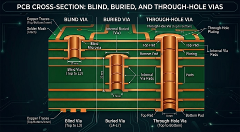
- Microvias and buried vias: Ultra HDI employs microvias—laser-drilled holes with diameters as small as 50 microns—connecting multiple layers of the PCB without requiring larger mechanical drill holes. This enables intricate, multi-layered structures that maximize space efficiency.
- Advanced material selection: High-performance materials are chosen for buildup layers to minimize mechanical stress during thermal expansion and aid signal integrity, particularly for high-frequency applications such as 5G, IoT, and high-speed computing.
There are many challenges with Ultra HDI fabrication and assembly, and many of these relate to the use of microvias in fine-pitch BGA fanouts. The use of small copper features and microvias is essential for working with higher-density components, as these features are required to route into fine-pitch BGA packages. The use of fine-pitch BGAs is another central feature of Ultra HDI builds, which makes these technologies the main enabler of smaller innovative products.

How Does Ultra HDI Differ from HDI?
While HDI technology already enables greater circuit density than conventional PCB designs, Ultra HDI takes it a step further. Here’s how:
- Finer Feature Sizes: HDI PCBs typically have trace widths and spaces around 50-75 microns, whereas Ultra HDI reduces these to 25 microns or less. This higher density means more routing possibilities within the same board space.
- More Advanced Via Structures: HDI designs use microvias, while the more advanced materials in Ultra HDI allow the use of stacked and staggered microvias with even smaller diameters. Thanks to CTE matching between copper films and Ultra HDI dielectrics, stacked microvias are less likely to experience failure than in traditional builds.
- Reduced Layer Count Versus HDI: Ultra HDI enables consolidation of signals onto buildup layers, so an Ultra HDI PCB can have fewer layers than the same design constructed as an HDI build.
These differences mean that Ultra HDI is not just an incremental improvement over HDI—it is a significant step forward that unlocks new possibilities for PCB designers working on next-generation products.
Why Is Ultra HDI Gaining Popularity?
The increased adoption of Ultra HDI is driven by the ever-evolving demands of industries that require cutting-edge electronics with high performance, compact form factors, and robust reliability. Here are some key reasons why Ultra HDI is becoming the go-to solution for advanced PCB design:
Miniaturization
The thin layers used in Ultra HDI PCB stackups allow designers to incorporate more components into a smaller space. These thin layers are also required to use very fine pitch BGA packages with small ball pitch.
Improved Thermal Management
With electronic devices generating more heat in increasingly compact spaces, thermal management is a crucial design consideration. Ultra HDI utilizes advanced materials that enhance heat dissipation, reducing the risk of overheating and improving device reliability.
Future of Next-Generation Technologies
Industries are shifting toward more complex and demanding electronic architectures, such as IoT, autonomous vehicles, and AI-driven systems. Ultra HDI technology ensures that PCBs are capable of handling higher processing speeds, greater data demands, and increased connectivity needs, making products more adaptable to future advancements.
What Does This Mean for PCB Designers?
For designers, Ultra HDI presents both new opportunities and challenges. While it allows for unprecedented levels of miniaturization and complexity, it also requires careful consideration in terms of layout, materials, and manufacturing processes. Design rules are more stringent, requiring a higher level of precision in component placement, via structures, and signal integrity management.
Additionally, designers must work closely with fabrication specialists to ensure manufacturability, as Ultra HDI demands cutting-edge fabrication techniques, such as laser drilling for microvias, advanced lamination processes, and highly controlled etching methods. Materials vendors also play an important role as they can recommend materials that are appropriate for certain applications and fabrication processes.
For PCB designers looking to stay ahead of the curve, mastering Ultra HDI is essential. Understanding its benefits, challenges, and implementation strategies will enable the development of next-generation electronic products that meet the needs of an increasingly sophisticated and compact digital world. As this technology continues to evolve, its adoption will likely become the new standard for high-performance electronic designs.


