What Are Ultra HDI and Package Substrates?


The printed circuit board industry is all abuzz about the CHIPS Act, as it should be. There are also many advocating for the CHIPS Act to include package substrate technology and ultra-high density interconnect technology. I couldn’t agree more! We need to look at the full supply chain for this endeavor to be successful. There has been a lot of activity around the ultra-HDI technology: fabricators are now easily providing trace width and space well below our traditional 3 mil line and space minimums and printed circuit board designers are navigating the learning curve of how to best take advantage of this ultra-high density capability. PCB technology that has not traditionally been available is now available in North America, at least in low to medium volumes.
Another product classification that must be considered is the package substrate market. This has traditionally only been produced outside of the United States and we are now fortunate that there are a few technology leaders in the printed circuit board space in the US that are investing in equipment and process improvements to allow them to supply to this market and provide a fully domestic solution for this supply chain.
One of the leaders in this technology is Averatek. Averatek is a technology development company that develops and licenses technology to the electronics industry. Their A-SAP™ product enables both ultra HDI and the ultra-fine features in the package substrate market. Their ELCAT™ process enables a next generation packaging solution including not just circuitry, but also embedded die. I had the opportunity to sit down with Mike Vinson, COO of Averatek, to discuss the Ultra HDI and package substrate market.
Tara: Hi Mike, can you help us understand the difference between these two technology areas?
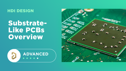
Mike: Package substrates, like HDI PCBs, use a variety of materials and techniques for this very broad market. We are primarily interested in organic substrates, that often are a miniature version of HDI PCBs. The materials are often chosen to reflect the characteristic requirements of the parts attached to the board, so often we see different materials for HDI and organic substrates, but many times the requirements are similar enough to allow for similar materials and techniques. There is even a category of substrate-like PCBs.
Tara: How are companies, including DoD and DoD primes with ITAR restrictions solving this supply chain issue today?
Mike: Today they are often forced to go overseas to find commercial shops with HDI and substrate capabilities. The domestic supply chain was decimated year by year, initially by low labor costs overseas and now by a concentration of industries that make for a completely vertically integrated solution.
Tara: When this technology is readily available in the US, what other industries do you think will lead the way to source in the US and which do you believe will continue to source from other areas?
Mike: Initially we will only see the markets that can realize a higher value from local manufacturing, like defense and medical, but once the infrastructure is established, automotive and industrial markets will soon follow. Evolving requirements in the information and communication infrastructure will eventually lead to restrictions that require local and trusted manufacturing. When final assembly of commercial products returns to the domestic market, PCBs will be ready.
Tara: How do Averatek’s A-SAP™ and ELCAT™ technologies benefit package substrate technology in the United States and for those already producing this technology outside of the US?
Mike: A-SAP™ is a technology that will enable a straightforward conversion from conventional to HDI/substrate markets that exceeds most requirements both domestically and overseas. ELCAT™ will provide a low-cost approach to packaging that previously only existed in expensive foundry environments.
Tara: What advice do you have for those new to this technology from a PCB design perspective?
Mike: A-SAP™ will add design flexibility and simplification due to reduced layer count and the routing freedom that higher density affords. Higher aspect ratios with vertical sidewalls of both space and trace will create more tightly coupled differential pairs and narrower traces will allow for thinner dielectrics on controlled impedance lines.
Tara: What advice to you have those new to this technology and considering investing in this from a fabrication perspective?
Mike: PCB requirements are changing. Look for technologies that will move you forward, both now and in the future. Identify the markets that will give good margins for exceptional performance and quality. Don’t settle for what is being currently done in the mainstream, leap ahead.
Tara: Thank you Mike. How do we contact you to discuss further?
Mike: You can visit our website at www.averatek.com or contact me directly at mike@averatek.com
Additional resources:
We have gone through the basics to SAP processing to look at some of the top questions related to the printed circuit board stack up. We have explored some of the “design rules” or “design guidelines” that do not change when designing with these ultra-high-density feature sizes. We've also looked at the design space around the possibility of utilizing these ultra-high density circuit trace widths in the BGA escape regions and wider traces in the routing field. The benefit is a reduction in circuit layers and the concern is maintaining 50-ohm impedance. Eric Bogatin recently published a white paper analyzing just this benefit and concern.


