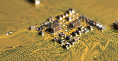


Capabilities for Ultra-High-Density PCB


Printed circuit board designers have an exciting new tool to use to help solve complicated routing challenges. Fabricators serving the low to medium-volume, high-mix markets are now offering Ultra-HDI technology, fabricating circuit layers with semi-additive processes. This gives PCB designers a number of key benefits: the ability to route with 25-micron trace and space with highly precise traces, the ability to use larger feature sizes with highly precise traces, improve controlled impedance tolerances, and the ability to use noble metals such as gold or platinum as the conductive metal to aid in biocompatibility for medical applications.
I recently had the opportunity to sit down with John Johnson, Director of Quality at American Standard Circuits (ASC). ASC is one of the first licensees of Averatek’s A-SAP™ process. This is a recap of questions asked and expert advice to help guide PCB designers as they start working with this technology.
What are your capabilities for ultra-high-density feature sizes today and what advancements does ASC have planned for 2023?
Today we have the ability to produce 25-micron features (1 mil lines and spaces) in a multilayer circuit board for FR-4, hybrid constructions, Flex and Rigid-Flex. In addition to standard ultra-fine line technology using copper traces, we can produce traces for medical applications solely from gold, palladium, and platinum.
In 2023 we will further advance our technology to build less than 25-micron features. Starting with circuitry in the 15 to 25-micron range, ultimately by the end of 2023 we should be able to reach 10-micron features.
What are the key design rules that a PCB designer should have in mind when starting their first design with ultra-fine feature sizes?
This is a great question. Today a designer has many options to use in their designs, but not all lend themselves to the Ultra-Fine line world.
When a designer is forced to use stacked microvias, via in pad plated over and subassemblies to route dense BGA components today, the ability to route with circuitry at 25 or even 50 microns gives the designer several advantages to consider. Typically, the first focus should be on using the line width advantage. Then look at reducing the number of levels of microvias by keeping use of a single level, or use of staggering vias and finally using stacked structures as a last resort. In doing so, the reliability advantage of simpler via structures can be realized.
If there is a benefit to using via in pad structures, plan to not use Ultra-Fine line circuitry externally. The process to produce Type VII via structures requires wrap plating and multiple plate ups which is not conducive to Ultra-fine lines. It still can be done, if required, but will increase costs of the design significantly. Consider the benefits of EMI shielding with the use of planes externally.
Externally, final finish is a concern if 25 micron space is involved. If possible, use solder mask defined pads or keep the fine line technology “under mask”. As an example, a requirement for 200 microinches of nickel in an ENIG finish can reduce a 25-micron space to 15 microns and potentially result in shorting.
What type of applications were the early adopters for the A-SAP™ process?
These have been in routing out of tight BGA’s, design simplification, RF needs and medical applications. Biocompatibility is especially suited to this technology.
You have a unique process serving the medical industry, can you explain the process using gold and other noble metals for a more fully biocompatible solution?
The biocompatibility needs of medical components are a unique factor. Copper and nickel are not biocompatible. How can a normal circuit board work without copper traces? Finishes need gold in most cases. But nickel is a base metal over copper to prevent copper migration.
The A-SAP™ process doesn’t need copper to function. It works from base laminate and builds up with Palladium and Gold to build circuitry. Other noble metals such as Platinum also can be employed. This eliminates copper and nickel in the build. Base dielectrics can also be biocompatible such as polyimide and LCP films.
ASC is also a leader in other technologies. What capabilities help you stand out in the PCB manufacturing industry?
ASC is a diversified manufacturer of many interconnect solutions. Metal core and metal backed boards, RF and hybrid RF boards using metal cores…or not. We also build High-density Multilayers up to 40 layers + using subassemblies, microvias, and buildup technologies. We offer high-density flex parts both double-sided and multilayer. Bookbinder constructions are available. Finally, Rigid Flex is another specialty in a variety of materials and builds.
How can readers get in touch with you with questions about how to best design for ultra-high-density features?
I can be reached at jjohnson@asc-i.com and our website is www.asc-i.com
Additional resources:
We have gone through the basics to SAP processing, recently looked at some of the top questions related to the printed circuit board stack up, explored some of the “design rules” or “design guidelines” that do not change when designing with these ultra-high-density feature sizes, and explored the design space around the possibility of utilizing these ultra-high density circuit trace widths in the BGA escape regions and wider traces in the routing field. The benefit is a reduction in circuit layers and the concern is maintaining 50-ohm impedance. Eric Bogatin recently published a white paper analyzing just this benefit and concern.
About Author
Related Resources
Related Technical Documentation
Table of Contents
- What are your capabilities for ultra-high-density feature sizes today and what advancements does ASC have planned for 2023?
- What are the key design rules that a PCB designer should have in mind when starting their first design with ultra-fine feature sizes?
- What type of applications were the early adopters for the A-SAP™ process?
- You have a unique process serving the medical industry, can you explain the process using gold and other noble metals for a more fully biocompatible solution?
- ASC is also a leader in other technologies. What capabilities help you stand out in the PCB manufacturing industry?
Design to Release, Without the Friction
- Keep reviews tied to the right version
- Reduce handoff confusion and rework
- Spot sourcing and release risk earlier
- Work solo, share when needed
Get Started
Thank you, you are now subscribed to updates.

