


How to Design Castellated Holes and Edges in a PCB for an SMD Module

At a Glance
Modules on small PCBs can be quickly surface-mounted to a carrier board with castellated holes. Here’s how you can design castellated edges.


SMD modules like the ESP32-WROOM or Raspberry Pi Pico microcontroller board use a particular mounting style called castellation PCB. If you look at these modules, it should be evident how castellated holes PCBs can be used to mount a PCB module as an SMD component. These small modules are becoming more popular and are simple to work with, but they might look a bit specialized for use in the standard PCB fabrication process.
While modules with castellated holes and additional holes for pin headers might not appear in the standard list of design objects in your CAD software, there's an easy method for placing an array of castellated holes on a module. Consider the fabrication process and potential assembly challenges. Using basic objects in your ECAD tools, you can efficiently place castellated holes on your PCB.
Castellated Edges in Your ECAD Software
Castellated holes are used on small modules as an alternative to pin-header mounting. Think about an Arduino hat or shield board form factor; instead of using pin headers to mate two boards, you can design the main board with castellated pads to mount an array of castellated holes.
This allows you to mate a small module, such as a Wifi expansion module or a motor driver module, to your main PCB with SMD soldering. Instead of using a pin header, using castellated holes on your module will provide a strong soldered connection between the module and your carrier board. To make this work, you need to design two arrays:
- Castellated holes array along the edge of your SMD module
- Pad array on the surface of your carrier board to hold your SMD module
Designing the Castellated Holes PCB Array on Your Module
Castellated holes come in two flavors. First, they can be placed as a half-hole along the edge with an attached pad. The other form of castellated holes includes a plated through-hole just inside the half-cut hole along the board edge. The typical arrangement of castellation PCB with the inner plated through-hole is shown below:

Here, you only need to use regular pads in your PCB layout tools to define an array of castellated holes. Simply line up your castellated pads with through-holes along the edge of the board, and then place another pad that runs right up to the edge of the board to provide additional copper onto the pad.
The second array of holes behind the board edge is optional, and you won’t find these holes on every SMD module that uses castellated holes. The 2nd row of holes can be designed to accept a pin header or small gauge wire. This is something you might do when you’re prototyping with a module or if you’re testing a module before mounting it on your carrier board. If you use a pin header, you’ll have to solder the header into the hole from the back side of the module. You also won’t be able to mount the module on your carrier board if you use too much solder. Keep this in mind if you’re considering using pin headers with a 2nd row of plated through-holes in a production castellated module.
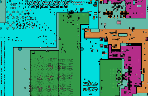
The image below shows an example of how these can be placed in your PCB layout tools. In this image, I’m halfway through designing a small module with an array of castellated holes along the board edge. Note that I’ve placed standard castellated pads with plated through holes, and the through holes hang over the edge of the board. This overhang can be addressed in fabrication.

Designing the Pad Array on Your Main Board
The pad array on the main board should follow standard land pattern design guidelines for other SMD components. Although the castellated holes will be treated as a through-hole feature in terms of soldering, these castellated holes can be soldered to a pad just like a typical through-hole component. After soldering, there will be a leftover solder fillet that is visible along the wall of the hole. SparkFun has a great tutorial on this, and the end result is shown below.

If you want to ensure reliability, or if you’re designing a high-reliability application that requires IPC Class 3 compliance, then there are some important points to consider when creating your castellated holes PCB array. Here, you need to design the pads on the main board so that they are large enough to accept the entire solder fillet. It’s also a good idea to use a small solder mask expansion around the pads (maybe ~4 mils on each side) to hold the molten solder and prevent bridging.
In addition, if you’re using a 2nd row of holes in your array, it’s important to place some solder mask in the region between the holes to create a solder dam. Do this on the pad for the carrier board as this is where the solder paste will be applied. This will prevent molten solder from wicking into the back hole.

Fabricating a PCB With Castellated Holes
Once you’ve placed the castellated holes onto your PCB, how do you get the bare board fabricated? The goal here is to ensure high quality and yield in a standard process, but Altium castellated holes PCBs do not seem to fit into the standard PCB fabrication process. Your fabricator can help you ensure your design will pass through fabrication by modifying the Gerbers to indicate drill hits and required plating along the board edge. This normally requires the following Gerbers (X2 format):
- Copper layers (GTL and GBL)
- Solder mask openings defined on both board surfaces (GTS and GBS)
- Drill files (TXT/DRL)
Some would say that the natural alternative to castellated holes PCBs is to just use solder pads to mount the module to your main board, just like any other SMD component. The main problem with this is the potential for contamination; the pad array on the carrier board can trap exhaust from some fluxes during reflow soldering. Another possibility is that excessive solder paste along the pad array lifts the module. This is similar to what can happen with SMD ICs that have a large ground pad in the center of the component.
When soldering a castellated holes PCB array, the solder fillet will be exposed during soldering. As long as the pad array on the main board is designed properly as described above, it’s a simple matter to apply solder paste and place the combined boards through reflow soldering, hand soldering, or selective soldering. You won’t have the potential for component liftoff or contamination from some fluxes during soldering.
With the best PCB design tools in Altium Designer®, you can easily create castellated edges in your PCB layout. You can also instantly create the fabrication files your manufacturer needs to correctly place your Altium castellated holes PCB array.
When you’ve finished your design, and you want to release files to your manufacturer, the Altium 365™ platform makes it easy to collaborate and share your projects. We have only scratched the surface of what is possible to do with Altium Designer on Altium 365. You can check the product page for a more in-depth feature description or one of the On-Demand Webinars.

About Author
Related Resources
Related Technical Documentation
Table of Contents
Design to Release, Without the Friction
- Keep reviews tied to the right version
- Reduce handoff confusion and rework
- Spot sourcing and release risk earlier
- Work solo, share when needed
Get Started
Thank you, you are now subscribed to updates.