Everything You Need to Know About Stitching Vias

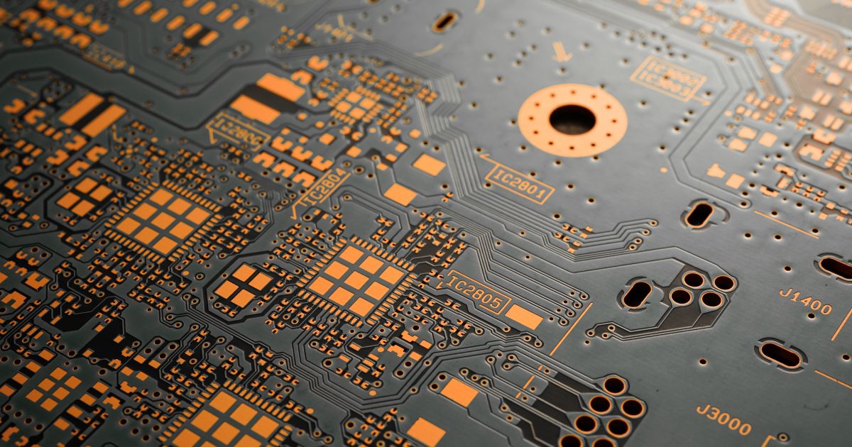
Stitching vias are something you often see spread around the surface layer of a PCB. If someone is using copper pour correctly, then they will ideally calculate an appropriate stitching via separation distance such that the via array suppresses crosstalk/interference. The other option is usage as multiple parallel connections between layers that can provide low resistance and impedance, and therefore they can provide high current in DC or AC.
In this guide, I’ll run over some of the standard uses of stitching vias and when they should be used in a PCB. This one area of PCB design can be contentious among some designers as it is related to copper pour, which it is often stated is not needed in most designs. Regardless of your feelings about copper pour, stitching vias have important uses in PCBs at low frequencies and at high frequencies.
The Basics of Stitching Vias in a PCB
Stitching vias are simple structures: they are a periodic array of vias that are generally grounded across the PCB stackup. In this way, they are making connections between ground nets on multiple layers. Note that there is one usage of via arrays that involves power connections across layers (see below). These structures also have important uses in RF design, and this sometimes causes stitching vias to be misused.
To get a quick look at some of the various ways stitching vias can be used in a PCB, watch the video below. Some of the major uses of stitching span across high-speed PCB design, RF PCB design, and routing power across multiple layers.
Let’s look at each of these uses in more detail:
The Typical Usage: Connecting Ground
The standard usage of stitching vias is to connect grounds across multiple layers. In a multilayer PCB, it’s common to have more than one region of copper assigned to the same ground net. Stitching vias are a useful tool for connecting these everywhere and ensuring minimum possible impedance for any return current propagating along the reference plane in the PCB.

Note that there is no requirement to use periodic stitching vias to make these connections across grounds. The grounds do need to be connected somewhere, and multiple connections may be preferable to ensure return paths are navigated to the power return point easily.
Layer Transitions Through Vias
This is one area where stitching vias connected to GND really show their value. Layer transitions in digital circuits and RF circuits need to have a clear ground reference to control signal propagation along an interconnect in a PCB. When making a layer transition, a nearby via in a stitching via array can perform the same function as the ground plane below a trace.
Generally, if you place a stitching via array in a PCB, there is likely to be a stitching via near a layer transition through a signal via. In some cases, this will probably work fine, and you probably won’t have to worry about the emission of noise or susceptibility to noise within the via transition region. The presence of a grounded stitching via near the signal via should be enough to suppress noise, particularly for slow GPIOs, I2C, UART, or other slow digital protocol (same applies in low frequency analog).

With high-speed digital and RF, the situation is different and you need to have a purposefully designed stitching via array near the signal via. The stitching via array is intended to provide a low-impedance path for the return current induced along the edge of the stitching vias. The other reason to place stitching vias in these transitions is to confine the electromagnetic field comprising this signal within the via structure bounded by the stitching via.

The noise-suppression mechanism in this case is sometimes called “shielding,” as if the vias prevent coupling of electromagnetic waves into a victim interconnect. This is somewhat true. Having the stitching via structure close to the signal via provides noise reduction in two ways:
- The loop inductance in the via region is lower because the via is closer to ground
- Being closer to ground causes the signal via/ground via transition to dominate the total capacitance experienced along the via

The 2nd point is equivalent to reducing parasitic capacitance by bringing a ground plane closer to a signal trace. I’ve shown how this reduces parasitic capacitive coupling to other signal nets in this article; the same kind of result would be expected here.
How Stitching Vias and Antipad Affect Via Impedance
Stitching vias and antipads work together to set the impedance of a via, both for single-ended signals and differential signals passing through vias. The modification of the capacitance and inductance in the previous section is that the placement of stitching vias in a layer transition will determine the via impedance. A related piece is the antipad, which ideally should intersect with the stitching vias, and thus together they will modify the impedance.
Most via impedance calculators are totally unable to account for the actual via impedance due to the presence of stitching via arrangements and the antipad size around a layer transition. The only way to accurately determine via impedance and the effect of stitching on via impedance is to use an electromagnetic field solver. We have to distinguish between the two types of stitching via options for single-ended and differential via transitions as shown in the table below.
Here we have two important conclusions about via impedance and stitching vias:
- For single-ended vias, stitching vias are needed to provide a return path, and thus they are the dominant factor setting the impedance of the via.
- For differential vias, stitching vias can affect the impedance, but the impedance is much more sensitive to antipad sizes and layer arrangement/Dk value on each layer.
Single-Ended Vias
Stitching vias surrounding single-ended vias impact both the impedance and localization (confinement of the electromagnetic field around the signal via). If you think about how these via transitions work, it should be obvious that the vias form a coaxial structure with the signal via at the center. The location of the vias would then determine the TEM mode cutoff in the via structure and the frequency at which the electromagnetic field begins to strongly radiate from the via structure (known as the localization frequency). The antipad size also impacts the localization frequency, but the most influential factor is the location and number of stitching vias.
The size of the antipad and location of the stitching vias also determine the input impedance looking through the via transition. In some stackups, the stitching vias may lie along the edge of the antipad, forming a partially connected ground connection which could be sensitive to drill wander. The example below shows such a via structure with the top-to-bottom and bottom-to-top curves marked in the graph (purple and red, respectively).
Differential Vias
In differential vias, the surrounding stitching vias are not required to ensure a defined return path. Instead, the stitching vias are required to set the localization limit and the TEM mode propagation limit around the vias. These factors in via design do not matter up to ~5 or 10 GHz, but for digital interfaces operating at 112G-PAM4 per lane and faster, stitching vias are incredibly important as they ensure TEM mode propagation up to frequencies beyond 28 GHz Nyquist and thus enabling data rates beyond 224G-PAM4 per lane.
The example below shows how adjusting the stitching via placement could affect a differential via. In the image below, I am comparing differential vias with merged circular antipads. The stitching vias are far from the signal vias. When we bring the stitching vias closer, we see that the localization frequency (green line) moves to a higher frequency, but there is no change in impedance. This means the stitching vias are playing a role in confining the electromagnetic field around the vias, but not much else.
The stitching vias in this case are not the strongest influence on capacitive loading of the differential pair at mid-range frequencies. The antipad and signal via-to-via spacing are already smaller than the stitching via distance, so they are the biggest determinants of capacitive loading.
When the signal vias have larger separation and when the antipad openings are larger, then the stitching vias will has a stronger influence on the signal via impedance because they could be a major source of capacitive loading. When the signal vias are closer together, the antipad is the greater determinant of the via impedance. When the signal vias are close together and the antipad is small, you may not notice any influence from the stitching vias (as shown above).
At low frequencies, don’t worry about how much stitching vias and antipad size affecting via impedance; you most likely won’t notice any effect because the via will be very electrically short. Above ~5 GHz, incorrectly placed stitching vias, large antipads, or no stitching vias might not provide enough capacitive loading, resulting in an inductive via transition with impedance reaching ~100's of Ohms up to a few dozen GHz.
Do Stitching Via Arrays Provide Shielding?
When placed in an array, the short answer is “yes,” but only up to certain frequencies. When used with the intent of providing shielding, it is possible that a designer just guesses at the required spacing between vias. In some cases, what we call shielding in waveguides should better be called field confinement. No matter what you want to call it, stitching vias can block propagation of electromagnetic waves up to some maximum frequency.
For a given frequency, that you want to suppress, the center-to-center pitch between the vias should be less than approximately:

Other guidelines will suggest different numeric factors in the denominator; I even recall seeing EMI/EMC guidelines with a factor 20 in the denominator. This spacing requirement on stitching vias specifically for purposes of blocking electromagnetic wave propagation is the same requirement used to confine waves within a waveguide on a PCB.
An example on a grounded coplanar waveguide used as an antenna feedline is shown below. In this example, the pitch is 20 mil, which would be appropriate for shielding up to 43 GHz based on the above equation. If we had high-speed signals traveling nearby, we could expect high shielding effectiveness along this feedline, and that would help suppress crosstalk into the RF line.

I think it’s important to note here that stitching vias are not the magic cure for noise, and they do not give you an excuse to eliminate best routing practices. You should still practice good placement and routing strategies for RF boards, even if you have used stitching vias in the manner shown above.
Stitching Vias for Power
When used in a PCB layout for a power system, stitching vias are not normally placed in the typical arrangement with large spacing. In fact, you may not see them used in large grounded copper pour regions at all in these designs. However, stitching via arrays can be used to create low resistance layer transitions on a power net. This would allow a via to transfer large amounts of current with low loss between layers.

How many stitching vias are needed to transfer a given amount of current? This depends on the DC resistance of the typical via. For a typical via drill diameter and pad size (10/20 mil) and 1 mil wall plating thickness, the via resistance will be approximately 1.5 mOhm, and the thermal resistance will be approximately 180 °C/W. If you attempt to bring 20 A DC through this via, you would dissipate 600 mW of power and you could expect the via’s temperature to increase by 108 °C.
In order to keep temperature rise within some acceptable limit, we would want to use multiple vias in an array. If we used 10 of these vias in parallel, then each via would carry 2 A DC and the expected temperature rise would be 1.08 °C for each via (and thus for the entire array). This should show how you can use a temperature rise target in order to determine a limit on the number of stitching vias.
Automate Stitching Via Placement
If we note that placement of stitching vias involves locating and placing a large array of vias around a board, and with precise spacing, this can be tough with most CAD tools. Simpler CAD tools force placement of stitching vias manually, probably followed by copy-pasting each row/column around the board to form the array.
Altium Develop includes a simple utility in the PCB Editor to place stitching vias with user-defined size and spacing. You can place stitching vias by selecting a via template, or by setting a custom via size and layer transition. This feature is accessible from the Tools menu inside the PCB Editor. Read more about this feature in the documentation.

So is there an objectively “right” way to use stitching vias? The answer is sometimes not so clear. I’ve shown some instances where stitching via arrays are used for very specific purposes:
- If you just need to connect grounds (no high-speed/RF), stitching vias are convenient but not required
- If providing a reference across layers, stitching vias are also convenient for low-speed signals to minimize EMI
- If providing power, closely spaced vias can provide high current with minimal temperature rise
- For high-speed signal transitions, you can’t rely on the randomly placed stitching vias to guarantee signal integrity
That leaves shielding as an outstanding issue regarding the sizing, spacing, and placement of stitching vias. To learn more, read this article on copper pour in PCB layouts to learn some of the effects of stitching vias on noise coupling and EMI.
Whether you need to build reliable power electronics or advanced digital systems, use Altium’s complete set of PCB design features and world-class CAD tools. Altium Develop provides the world’s premier electronic product development platform, complete with the industry’s best PCB design tools and cross-disciplinary collaboration features for advanced design teams. Experience Altium Develop today!


