


High Density Interconnects - A Design and Manufacturing Guidebook

At a Glance
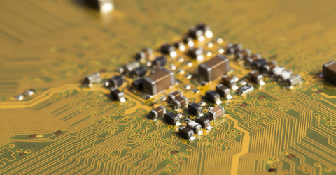
A compilation of Happy Holden's expert advice on high density interconnect design, routing, layout, and manufacturing for HDI PCBs.


CHAPTER 1
Introduction to High Density Interconnects
THE EVOLUTION OF ELECTRONICS
Electronics is a relatively new industry, since it has been only 65 years since the transistor was invented. The radio tube was developed nearly 100 years ago but blossomed in WWII, with communications, radar, ammunition fusing (especially the radar-altimeter electronic fusing for the first atom bomb) and has evolved into the world largest industry. All electronic components must be interconnected and assembled to form a functioning unit. Electronics packaging is the technology where we integrate the design and manufacturing of these interconnections. Since the early 1940s, the basic building platform of electronic packaging is the printed circuit board (PCB). This Guidebook outlines the advance design approaches and manufacturing processes needed to design the most complex of these PWBs, the high-density interconnects (HDI), as illustrated in Figure 1.
This chapter introduces the basic considerations, the main advantages, and the potential obstacles that must be accounted for in the selection of the highdensity interconnection methods. Its main emphasis is on the interconnections and wiring of components. The focus is on density and the potential effects that the selection of various HDI board types and design alternatives could have on the cost and performance of the complete electronic assembly.
As printed circuits became more commonplace since the early 50s, the density and complexity of interconnects has increased quickly, but not as much as the last ten years. Conventional printed circuit technology is capable of meeting most of today’s requirements. Yet, there is a growing group of products referred to as “High Density Interconnects” (HDI for short) that are used to create still denser interconnect, and it is these that are the subject of this Guidebook.
Interconnect Trends
Interconnect Trends Drivers for higher-density interconnection come under three headings; platforms, performance and parts:
Platforms
With fast-growing markets for products such as mobile phones, digital appliances and wearable computers, all of which represent new opportunities. HDI makes possible electronics becoming smaller and lighter.
Performance
With decreased semiconductor rise-times, and more RF and microwave communications, at frequencies up to 80 GHz in some telecom’s areas.
Parts
The evolving silicon technology of smaller transistors and its faster rise-times leads to the challenge to provide more leads in a smaller footprint, which equates to more connections per unit area.
All these trends create a demand for denser interconnects, with smaller trace and gap dimensions, smaller vias, and more buried vias. While this is not necessarily accompanied by a change in board design practices, conventional constructions can reach their limits and the design of HDI constructions require rethinking of design strategies.

FIGURE 1. Electronics have evolved in density from the 1940’s, to the current state of high-density interconnects that include 3D stacking and embedded components.
HDI MULTILAYER PLATFORMS
HDI is such a large and growing PWB application market, that there are at least three (3) different HDI Platforms that make it up. These four platforms are 1. Substrates & Interposers modules; 2. Portables; and 3. High performance.
Substrates & Interposers Modules
This technology is used for flip chip or wire bondable substrates. Microvias allow the increased density needed to escape from the high-density flip chips. The dielectric materials are the newer engineered films. A typical example is seen in Figure 2. The modules are small substrates that may have their ICs wire bonded, flipchipped or TAB mounted or may use fine-pitch CSPs. The discrete components are typically very small, like 0201 or 01005s and may even be embedded. The design rules are usually coarser than the single IC substrate, since the module may be larger than a single IC package.
Portables
Portables and miniaturized consumer products are the leading edge in HDI Technology. The dense designs offer small form factors and very dense features including micro-BGA and flip chip footprints. The largest application is currently mobile phones. A typical mobile phone product (Motorola MicroTack and the Apple iPhoneX) are seen in Figures 3.
High Performance
This technology is used for high layer count boards with high I/O or small pitch components. A buried via board is not always necessary. The microvias are used to form the escape area of dense components (high I/O, micro BGA). Dielectric is reinforces-resin coated foil, reinforced prepregs and cores and high-performance laminates. A Typical example is seen in Figure 4. A possible 4th platform to be developed is ‘embedded components’ seen in Figure 5.

FIGURE 2. High-density modules for a. Flip chip substrates and b. Telecom

FIGURE 3. Ever increasing complexity and density characterize the HDI boards used in mobile phones from 1994 through the present day.

FIGURE 4. A high reliability telecom board for a triple OC-192 (10 Gb/s) optical network controller. Construction is of low-loss laminates and uses a 1+6+1 HDI structure.

FIGURE 5. The typical usage of microvias to connect various embedded capacitors and Resistors.
PERFORMANCE IMPROVEMENTS
When performance improvements are required for PWBs, HDI is the leading contributor. In additions to making the PWB smaller, lighter and thinner, it will have superior electrical performance. Some of these improvements are:
- Order of magnitude lower via electrical parasitic
- Minimal stubs
- Stable voltage rail
- Removal of decoupling capacitors
- Lower crosstalk and noise
- Much lower RFI / EMI
- Closer ground planes
- Opportunities for distributed capacitance (PWR/GND)
- Surface ground planes w/via-in-pads cut emissions and radiation
As semiconductor fabs reduce the size of their devices, the physics allows faster rise / fall times. This manifests itself in higher-frequency performance. But with smaller devices comes many more on a chip and higher heat dissipation. With a reduction in power supply voltage to minimize the power dissipation, what results is to increase the sensitivity of circuits to various forms of noise and loss of signal strength. High-performance laminates have always been one of the requirements. Additionally, improved processes for microvias fabrication also improve high-frequency performance. Microvias have nearly 1/10 the parasitics of THs. Test Vehicle structures can validate the lower inductance in microvias, and when combined with low-inductance decoupling capacitors, and via-in-pads, show the merits of noise reduction, especially for high-speed logic.
ACCESS TO ADVANCED COMPONENTS (PARTS)
The semiconductor industry is the primary driver for electronics. Smaller gate geometries and greater total gates allow more functions to be performed – and faster. With larger wafers, the prices continue to tumble.
IC packaging, say a 0.80- and 0.65-mm. pitch device, benefit from PCB technologies like HDI, but the use of 0.8 mm pitch and smaller devices is where HDI really begins to provide advantages. The blind vias save room on inner layers and have reduced via lands, as well as making possible via-in-pads. Typical of these devices is the 953 pins, 0.65mm pitch, Digital Signal Processor (DSP) seen in Figure 6a or the 498 pins DSP shown in Figure 6b. The other new components becoming more widespread are ones with very high pin counts of around 600 to 2500 pins, even at 1.00- and 0.8-mm pitches. Although some of these are telecom digital switches (Figure 6c), the vast majority are the new field programmable gate arrays (FPGAs). Current products from Actel, Infineon, Xilinx and Altera have packages with 456, 564, 692, 804, 860, 996, 1020, 1164, 1296, 1303, 1417, 1508, 1696 and 1764 pins. FPGAs of greater than 2000 pins are being designed!

FIGURE 6. a. Fine-pitch devices such as these 953 pins - 0.65 mm pitch microprocessor, b. the 498 pin 0.5mm DSP device or c. the 480 pin @ 0.4 mm controller, even the d. 182 pins @ 0.25 mm require microvias. e. The 2577 pin - 1.0 mm pitch digital switch now require microvias in order to connect them on a printed circuit.
HDI OPPORTUNITIES
Other benefits of using HDI technologies can come from the ease of design resulting in Faster Time-to-Market and its Improved Reliability.
Faster Time-to-Market
The faster time-to-market comes about because of easier placement of components using blind vias or via-in-pads. Other design efficiencies come about because of smaller spacing, improved BGA breakouts, boulevards routing (see Chapter 4), and ease of autorouting using blind/buried vias over through-hole vias. The overall system design times can be reduced because of the improved electrical performance of blind vias instead of TH vias, fewer respins will be required because of signal integrity and noise reduction.
Improved Reliability
Extensive reliability testing was performed by the IPC-ITRI in the late 1990’s about the reliability of microvias. [1] Other groups (like HDPUG & NASA-JPL) have also produced reports on the superior reliability of small-blind vias over TH vias. [2] Understanding ‘WHY’ is quite simple! The via aspect ratio (AR-depth to diameter ratio) is less than (<) 1:1 compared to TH with an AR of >6:1 (+) that go as high as 20:1. This is a result of the thin materials and low Z-Axis TCE materials used in HDI (see Chapter 2). HDI materials are numerous and exceed multilayer laminate in variety, thus they are covered by the IPC Standard IPC-4104A and not IPC-4101B. If the blind vias are properly drilled and plated, then they will perform with many times the thermal cycle like typical THs (see Chapter 6)
The thin HDI materials are thus well suited for thermal heat transfer and this is also covered in the IPC HDI Design Standards, IPC-2226.
Lower Cost
Chapters 4 and 5 will discuss in detail, the improved design process for HDI PWBs. Properly planned and executed, HDI multilayer can be less expensive than the TH board alternative. As illustrated in Figure 4, the Benchmark of a high-speed, controlled impedance 14-layer TH multilayer to an 8-layer HDI multilayer. By fully utilizing the Secondary Side of the PWB, 40% less area was required to connect all the components, in addition to 6 less layers.
PREDICTABILITY OR “WHAT WILL IT COST?” AND THE NEED FOR DESIGN MODELS
Predictability
Customers need to know the HDI stackup, design rules and PRICE, BEFORE starting the project or board design.
Fabricators can quote the design AFTER it is designed, but without the numbers up front - no one can afford the time to run down a blind alley. The concept that, “Microvias cost more!” is one of not knowing how to properly design an HDI board.
One of the benefits of Benchmarking HDI for the last 37 years, was the TH versus HDI Trade-Off chart seen in Figure 7. The Price / Density Comparison. The two key variables are RCI, a comparison currency, normalized to the actual price of an 8-layer multilayer and DEN, the average number of pins on a board divided by the length and width of the board.

FIGURE 7. TH versus HDI Price / Density Comparison. The Relative Cost Index (RCI) and DENsity predictor (pins/sq. inch) provides a quick comparison of TH layers (column A) to equivalent HDI structures (columns B – G).
The RCIs in the matrix is the ‘Basis’ numbers (or minimums) for costs. But the ‘Ceiling’ number for a range is out of our ability to calculate or set up at this time. It all depends on the various factors in the design. Yields are very sensitive to min. diameter, annular rings, min. trace and spacing, material thicknesses, total number of holes and their density. Other cost factors such as final finish, hole filling, and tolerances will affect the price. I have added a column for “Density” (DEN). This is the Maximum Number of Electrical Connections (called ‘pins’) per square inch of surface (for both sides). The dashed lines are “Equivalent” PCBs. So, as an example, an 18-Layer TH (through-hole-column A) board with an average of 100 ‘pins’ per sq. in could have been designed as a 10-layer HDI board (1+8+1-column C) because it can handle 210 ‘pins’ per sq. in (p/si). Or, it could have been designed as a 6-layer HDI board with 2+2+2 (column E, also 200 p/si).
The RCI does not show the “Absolute” cost savings in this example. The “Relative” cost saving is 28.1% for the 10-layer and 20.5% for the 6-layer HDI ‘equivalents’. But a smaller board could result in more boards per panel and the ‘PRICE” would be even lower than the above numbers. In the range of 8L to 18L, the HDI boards, especially the 2+N+2 are NOT the equivalent of 8L to 18L TH boards, they represent boards with 12X- 20X the density of TH boards.
This Matrix is based on FR-4. This has two important implications. The TH RCI scale (from 4L – 16L) represents competitive pricing set by China. This scale is depressed compared to the HDI pricing. So the HDI pricing, if equal or lower, is very competitive. If the material of construction is NOT FR-4, but a more expensive, low Dk or low Dj material, then the savings from HDI will be MUCH LARGER as you reduce layers!
CHAPTER 2
MATERIALS FOR HIGH DENSITY INTERCONNECTS (HDI)
In this chapter, we will discuss the materials used to manufacture HDI circuits. Several good resources exist on the subject of materials for PCBs (such as the Printed Circuit Handbook edited by Holden & Coombs), so we will concentrate on those materials that are specific to HDI.
The current HDI materials market worldwide was estimated by BPA Consulting Ltd. to be 83 million square meters. The breakdown by BPA Consulting of the eleven (11) HDI materials used, in order of usage:
- Laser-Drillable Prepregs-40.4%
- RCC-28.3%
- Conventional Prepregs-17.2%
- ABFilm-5.0%
- Epoxy-3.3%
- Other-3.2%
- BT-1.8%
- Aramid-0.4%
- Polyimide-0.3%
- Photo Dry film-0.1%
- Photo Liquid-~0.0%
The major material components of PCBs are the polymer resin (dielectric) with or without fillers, reinforcement, and metal foil. A typical construction is shown in Figure 1. To form a PCB, alternate layers of dielectric, with or without reinforcement, are stacked in between the metal foil layers.
The majority of the materials are epoxy, but some are BT, PPE, cyanate ester, and modified acrylates. The newest materials are the growing number of laser-drillable prepregs.

FIGURE 1. Construction of a PWB laminate [Source: PC Handbook,7th Ed]
DIELECTRICS AND INSULATORS
The backbone resin of the industry has been the epoxy resin. Epoxy has been a staple due to its relatively low cost, excellent adhesion (both to the metal foils and to itself), and good thermal, mechanical, and electrical properties. As demands for better electrical performance, ability to withstand lead-free solder temperatures (see Table 1), and environmental compliance have entered the picture, the basic epoxy chemistry has been dramatically changed over the years.
Epoxies are thermosetting resins and use hardeners and catalysts to facilitate the cross-linking reactions that lead to the final cured product. Epoxies are also inherently f lammable, so flame retardants are incorporated into the resin to greatly reduce the flammability. Traditionally, the main curing agent was Dicy, but now various phenolic compounds are used. The traditional bromine compounds (i.e., TBBA) used as flame retardants are being substituted with other compounds such as those containing phosphorus because of concerns about bromine getting into the environment when the PCBs are disposed of. Many companies have gone to a “HalogenFree” requirement in anticipation of an eventual ban or for the appearance of being “green.”

TABLE 1. The four important thermal characteristics of a ‘lead-Free’ laminate and STII.

FIGURE 2. Some STII values of common laminates.
Other resins that are in common use are typically selected to address specific shortcomings of epoxy-resin systems. BT-Epoxy is common for organic chip packages due to its thermal stability, while polyimide and cyanate ester resins are used for better electrical properties (lower Dk and Df) as well as improved thermal stability. Sometimes they will be blended with epoxy to keep costs down and improve mechanical properties. An important thermal property for lead-free assembly is the STII and some laminates values are seen in Figure 2.
Besides thermosetting resins, thermoplastic resins are utilized including polyimide and polytetrafluoroethylene (PTFE). Unlike the thermoplastic version of polyimide which is relatively brittle, the thermosetting version is flexible and is supplied in film form. It is typically used to make flexible circuits as well as the combination circuits called rigid-flex. It is also more expensive than epoxy and is only used as needed.
To aid in your selection of the proper laminate for HDI, Figure 3 shows a selection of laminates from around the world and their equivalency.

FIGURE 3. Laminate substitution chart for many PCB laminates
REINFORCED MATERIALS
Laser-Drillable and Conventional Fiberglass
Most of the dielectric materials that are used to make printed circuit boards incorporate reinforcement into the resin system. Reinforcement usually takes the form of woven f iberglass. Woven fiberglass is just like any other cloth, made up of individual filaments that are woven together on a loom. By using different diameter filaments and different weave patterns, different styles of glass cloth are created.
Fiberglass adds both mechanical and thermal durability to the dielectric, but it does present some problems when used in HDI constructions. Figure 5 shows that glass fabric is woven, and the table shows the styles, yarns, and thicknesses of those yarns. When lasers are used to create the vias, the difference in ablation rates between the fiberglass and the surrounding resin can cause poor hole quality. Also, since the fiberglass cloth is not uniform due to having areas with no glass, areas with one strand, and the intersections of strands (also known as knuckles), it is difficult to set up drilling parameters for all these regions. Usually the drilling is set up for the hardest to drill region which is the knuckle area.
The fiberglass manufacturers have created so-called laser-drillable dielectrics by spreading the yarns in both directions and making the fabric more uniform which minimizes the areas with no fiberglass as well as the knuckle area. Figure 4 shows the 12 currently available LDPs and their properties. It still takes more energy to penetrate the fiberglass than the resin, but now the drilling parameters can be optimized to get consistent results throughout the panel.

FIGURE 4. Table of cloth specifications for laser-drillable fiberglass.
RCCs
Resin Coated Copper (RCC) Foil
The limitations of fiberglass-reinforced dielectrics prompted companies to look at alternative dielectric solutions. In addition to the problems with laser drilling (poor hole quality and long drilling times), the thickness of woven fiberglass limited how thin the PCBs could be. To overcome these issues the copper foil was utilized as a carrier for the dielectric so it could then be incorporated into the PCB. These materials are called “Resin Coated Copper’ or RCC. RCC foil is manufactured using a roll to roll process.

FIGURE 5. Photos of standard and laser-drillable fiberglass cloths
The copper goes through a coating head and the resin is deposited on the treated side of the copper. It then goes through drying ovens and is partially cured or “B” staged which will allow it to flow and fill in the areas around the internal circuitry and bond to the core. The resin systems are usually modified with a flow restrictor to prevent excessive squeezeout during the lamination process.
Most of the RCC foil is manufactured this way, but additional types exist. One of these types is a two-stage product (Figure 6 ). After the first resin layer is coated, it is put through the coater again to add a second layer. During the second coating the first layer is fully cured, while the second layer is “B” staged. The benefit of this process is that the first stage acts like a hard stop and guarantees a minimum thickness between layers. The disadvantage is that the product is more expensive than the single coated version.
For all the benefits of RCC foil, there are concerns over the lack of reinforcement in terms of dimensional stability and thickness control. A new material was developed to address these concerns. MHCG from Mitsui Mining and Smelting incorporates an ultrathin fiberglass (either 1015 or 1027) during the resin-coating process. The fiberglass is so thin that it cannot be made into a prepreg since it cannot go through a treater tower like traditional fiberglass. There is also a polyimide / epoxy RCC available.
The fiberglass does not impact laser drilling significantly, yet it provides dimensional stability equal to or better than standard prepreg. Dielectric layers as thin as 25 microns are now available allowing for very thin multilayer products.
Cost is another aspect of RCC foil that is of concern. RCC foils almost always cost more than the equivalent prepreg/copper foil combination. However, the RCC foil can actually result in a less expensive product when laser-drilling time is taken into consideration. As the number of holes and size of the area increase, the improved throughput of the laser drills more than offsets the increased cost of the RCC foil.

FIGURE 6. Four available styles of resin coated copper (foil)
OTHER DIELECTRICS
Optimized liquid epoxy can provide the lowest cost of any of the dielectrics for HDI. It is also the easiest to apply in thin layers for fine-line wiring. It can be coated by screen printing, vertical or horizontal roller-coating, meniscus coating, or curtain-coating. The Taiyo Ink brand is the most used but Tamura, Tokyo Ohka Kogyo, and Asahi Denka Kogyo also have products.
Polyphenyl Ethers/Polyphenylene Oxide: M.P > 288° C are thermoplastics of Polyphenyl Ethers (PPE) or Polyphenylene Oxide (PPO) with melting points well over 288°-316° C. PPO/Epoxy blends have a Tg >180° C with higher decomposition temperatures. Their popularity is their excellent electrical performance due to having lower dielectric constants and loss tangents than many of the thermosets like epoxy and BT with low water absorption. Their high melting points and chemical resistance make desmearing a critical process.
ELECTRICAL PROPERTIES
Figure 7 displays the dielectric constants (Dk) and dissipation factors (Dj) of popular dielectrics, including those suitable for very high-speed logic. Table 2 lists other electrical characteristics related to high-speed performance for HDI design.

FIGURE 7. The electrical characteristics of various laminates by their dielectric constant and dissipation factor

TABLE 2. Other important electrical performance considerations when designing high-speed circuits.
ENABLING FINE TRACES AND SPACES
For very high-speed logic, the signals travel on the surface of the conductor (the Skin Effect). Smooth copper foils enable the fabrication of very fine traces and spaces with less copper losses. (See Figure 8) in Figure 9, ultra-fine traces are capable with the 5 micron and 3 micron copper foils, or with a mSAP process.

FIGURE 8. Foil treatment for adhesion comes in four profiles and is important for copper losses (skin effect)

FIGURE 9. Very thin and smooth copper foil can permit very fine traces and spaces (8um/8um)
Materials for High Density Interconnects is a serious subject for PCB designers and Electrical Engineers. Several good resources exist on the subject of materials for PCBs and the focus here has been HDI Materials to help the engineer design printed circuit boards.
CHAPTER 3
HDI Manufacturing Process
INITIAL HDI FABRICATION
High Density Interconnect printed circuits actually started in 1980, when researchers started investigating ways to reduce the size of vias. The first innovator is not known, but some of the earliest pioneers include Larry Burgess of MicroPak Laboratories (developer of LaserVia), Dr. Charles Bauer at Tektronix (who produced photodielectric vias), [1] and Dr. Walter Schmidt at Contraves (who developed plasma-etched vias.
The first production build-up or sequential printed boards appeared in 1984, starting with the HewlettPackard laser-drilled FINSTRATE computer boards, followed in 1991 in Japan with Surface Laminar Circuits (SLC) [2] by IBM-YASU and in Switzerland with DYCOstrate [3] by Dyconex. Figure 1 shows one of those first Hewlett Packard FINSTRATE boards, on the cover of Hewlett-Packard Journal (1983).
HP Finstrate Laser-Via
HP did not intend to develop laser-drilled microvias. They were the result of reverse-engineering their new 32-bit microcomputer chip. They called it the “FOCUS” chip, a 32-bit microprocessor developed in NMOS-III, which has the characteristic of being very current-hungry. One of the early surprises with this new microprocessor was that it could not drive the inductance of a standard 0.3 mm dia. through-hole via in a 1.6 mm thick board. It could only drive 20-30 nHenrys of inductance, or a blind via of 0,125mm. The second surprise was that it did not have the energy to drive the normal losses of FR-4 (Dj=0.020), so pure polytetrafluoroethylene (PTFE) was used. The IC requirement for cooling required a metal-core board with very tiny blind-vias and a very low-loss dielectric. The resulting board created was a copper-core, buildup technology that had direct wire-bonded integrated circuits (ICs).

FIGURE 1. The first microvia PCB in general production. Hewlett Packard’s FINSTRATE was put into production in 1984. It was a copper-core, build-up technology with pure PTFE as a dielectric that had direct wire-bonded integrated circuits (ICs).
IBM SLC Photo-via
Since the introduction of IBM’s SLC technology in 1991, many variations of methods for mass-producing HDI wiring boards have been developed and implemented, judged in terms of volume produced, laser-drilling technology is the one. Other methods are still used by a number of PWB manufacturers, but on a much smaller scale.
However, a greater emphasis will be placed on the laser-drilling process (laser via hereafter) since it is the most popular process today and it seems that its popularity will grow in the future. It must be understood that via hole formation is just one element of fabricating HDI wiring boards. Fabrication of HDI wiring boards with microvia holes involves many processes not common to conventional board fabrication.
HDI Fabrication Basics
Figure 2 shows the breakdown of Sequential Build-Up Technologies (SBU) or High Density Interconnects manufacturing process. The three basic elements are:
- Dielectric Format
- Via Formation
- Metallization Methods

FIGURE 2. Sequential build-up technology (HDI) has three major characteristics: Dielectric Format, Via Formation, and Metallization Methods (Courtesy of DuPont.)
The manufacturing process for each microvia technology begins with a base core, which may be a simple double-sided board carrying power and ground planes, or a multilayer board carrying some signal pattern in addition to power and ground planes. The core usually has plated through-holes (PTHs). These PTHs become BVHs. Such a core is often called an active core.
Dielectrics and Insulators
An overview of the dielectric and applied conductive materials used in microvia fabrication are covered in IPC-4104A standard. Some of these dielectrics can be used in both chip packaging and PWB HDI applications. Cross-references are made to the relevant material specifications of the IPC/JPCA-4104 specification for HDI and microvia materials.
Material selection needs to answer these questions:
- Will the dielectric use chemistry compatible with current chemistry used by core substrate material?
- Will the dielectric have acceptable plated copper adhesion? (Many original equipment manufacturers [OEMs] want >6 lb./in. [1.08 kgm/ cm] per 1 oz. [35.6 µm] copper.)
- Will the dielectric provide adequate and reliable dielectric spacing between metal layers?
- Will it meet thermal needs?
- Will the dielectric provide a desirable “high” Tg for wire bonding and rework?
- Will it survive thermal shock with multiple SBU layers (i.e., solder floats, accelerated thermal cycles, multiple reflows)?
- Will it have platable, reliable microvias (that is, will it have latitude to ensure good plating to the bottom of the via)?
- Material selection needs to answer these questions:
- Will the dielectric use chemistry compatible with current chemistry used by core substrate material?
- Will the dielectric have acceptable plated copper adhesion? (Many original equipment manufacturers [OEMs] want >6 lb./in. [1.08 kgm/ cm] per 1 oz. [35.6 µm] copper.)
- Will the dielectric provide adequate and reliable dielectric spacing between metal layers?
- Will it meet thermal needs?
- Will the dielectric provide a desirable “high” Tg for wire bonding and rework?
- Will it survive thermal shock with multiple SBU layers (i.e., solder floats, accelerated thermal cycles, multiple reflows)?
- Will it have platable, reliable microvias (that is, will it have latitude to ensure good plating to the bottom of the via)?
There are nine different general dielectric materials used in HDI substrates. IPC slash sheets like IPC-4101B and IPC-4104A cover many of these, but many are not yet specified by IPC standards. The materials are: There are nine different general dielectric materials used in HDI substrates. IPC slash sheets like IPC-4101B and IPC-4104A cover many of these, but many are not yet specified by IPC standards. The materials are:
- Photosensitive Liquid Dielectrics
- Photosensitive Dry Film Dielectrics
- Polyimide Flexible Film
- Thermally Cured Dry Films
- Thermally Cured Liquid Dielectric
- Resin Coated Copper Foil (RCC), dual-layer and reinforced
- Conventional FR-4 Cores and Prepregs
- New ‘spread-glass’ laser-drillable (LD) Prepregs
- Thermoplastics
Interconnect Via Formation
This section discusses processes that employ various drilling via-hole formation techniques. Through-via drilling is possible below 0.20 mm (0.008 in.), but cost and practicality discourage this. Below 0.20 mm (0.008 in.), laser and other via-formation processes are more cost-effective. There are many different methods of forming the IVHs used in HDI processes. Laser drilling is the most prominent. These different methods of via formation have some limits on the minimum size of the vias they form, as well a significant differences in rate of via formation.
Mechanical Drilling
The oldest technique for blind and buried via formation is mechanical drilling and sequential lamination, as seen in Figure 3a and 3b. Progress has been made in both small drill-bit manufacture and high-speed mechanical drilling to allow this technique to be used in some circumstances.

FIGURE 3. Mechanically drilling the small vias by either controlled depth, Figure 3a, or sequential lamination, Figure 3b, is how HDI started in volume production.

FIGURE 4. Creating the blind-via in a PWB panel is normally done with laser technology but ‘mass via processes’ like chemical etching, plasma or photo dielectrics have also been used.
Laser Via Technology
Laser via processing is by far the most popular microvia hole formation process. But it is not the fastest via formation process. The chemical etching of small vias is the fastest, with an estimated rate of 8,000 to 12,000 vias per second. This is also true of plasma via formation and photovia formation (Figure 4). These are all mass-viaformation processes. Laser drilling is one of the oldest microvia generation techniques. [1] The wavelengths for laser energy are in the infrared and ultraviolet region. Laser drilling requires programming the beam fluence size and energy. High-fluence beams can cut metal and glass, whereas low-fluence beams cleanly remove organics but leave metals undamaged. A beam spot size as small as approximately 20 microns (<1 mil) is used for high-fluence beams and about 100 microns (4 mil) to 350 microns (14 mil) for low-fluence beams. [2] [3]
Most laser processes utilize either CO2 or UV lasers since they are the most readily available and economical lasers. When using a CO2 laser to produce vias in epoxy laminates, the copper must be removed above the area to be ablated (See Figure 5). The CO2 laser is primarily used for laminates not supported by glass. This includes unsupported laminates such as flexible polyimide and resin-coated copper (RCC®) foil and laminates reinforced with alternative materials such as aramid fibers. The modified TEA CO2 (Transversely Excited Atmospheric) lasers are specifically created to laze through glass fibers using 9,000 nm wavelength and higher peak power.
However, there are many variations. For the purpose of drilling microvia holes, there are five laser systems: UV/ Eximer, UV/Yag laser, CO2 laser, Yag/ CO2, and CO2/ TCO2 combinations. There are also many dielectric materials: RCC, resin only (dry film or liquid resin), and reinforced prepreg. Therefore, the number of ways to make microvia holes by laser systems is driven by the permutation of five laser systems and these dielectric materials, as seen in Figure 5.
Higher power lasers (i.e. Ultra Violet-UV) can remove glass and copper and can therefore be used with conventional laminates, but are typically slower when going through copper and glass fibers. There are several factors to consider in laser via processing: position accuracy of lasered holes (microvia holes), uneven diameters of holes, and dimensional change of the panel after curing dielectric, dimensional change of the panel due to temperature and humidity variations, alignment accuracy of the photo-exposure machine, unstable nature of negative artwork, and so on. These should be carefully monitored and are important for all microvia hole processes.

FIGURE 5. The three main laser blind-via ablation processes; c. lasing open the window in copper foil using UV or special treatments with CO2 lasers; d. Etching open a window in the copper foil and then lasing the dielectrics; e. Eximer lasing the via in materials and then metaling the dielectric with sputtering or electroless copper mSAP.
Method of Metallization
The last process is metallization of the vias. There are four different methods of metallizing the IVHs used in HDI processes. The methods are:
- Conventional Electroless and Electroplating Copper
- Conventional Conductive Graphite or other Polymers
- Fully and Semi-Additive Electroless Copper
- Conductive Pastes or Inks (Figs. 6f and 6g)
The laser is the most common method of production of microvias to be filled with a conductive paste. Lasers are capable of ablating dielectric material and stopping when intercepting the copper circuitry, so they are ideally suited for creation of depth-controlled blind vias. Figure 6 shows these two major microvia processes.

FIGURE 6. Two of the most popular Asian processes for micro-via hole metalization is with conductive polymers; f. The BBiT process screens a conductive silver paste on copper foil and laminates it into the 2-sided core; g. Various conductive pastes are screened into laser-drilled holes in the b-stage dielectric and then laminated with copper foil into the core.
CHAPTER 4
Design Baiscs for HDI
DEFINING INTERCONNECT DENSITY
When planning an HDI design, there are measures of performance or metrics for the HDI process. Like the triangle in the Figure 1, these three vital chains of the HDI Process are elements of interconnection density.

FIGURE 1. HDI Design Metrics
ASSEMBLY COMPLEXITY
Two measures of the difficulty to assemble surface mounted components, Component Density (Cd),measured in parts per square inch (or per square centimeter) and Assembly Density, (Ad), in leads per square inch or per square centimeter.
COMPONENT PACKAGING
Two measures of the difficulty to assemble surface The degree of sophistication of components, Component Complexity, (Cc), measured by its average leads (I/Os) per part . A second metric is component lead pitch.
PRINTED WIRING BOARD DENSITY
The amount of density (or complexity) of a printed circuit, Wd, as measured by the average length of traces per square inch of that board, including all signal layers. The metric is inches per square inch. or cm per square centimeter. A second is the number of traces per linear inch or per linear cm. The PWB density was derived by assuming an average of three electrical nodes per net and that the component lead was a node of a net. The result was an equation that says the PWB density is times the square root of the parts per square inch times the average leads per part. β is 2.5 for the high analog/ discrete region, 3.0 for the analog/digital region and 3.5 for the digital/ASIC region:
PWB Density (Wd) = β √ [Cd] x [Cc]
= β √ [parts per sq. in.] x [ave.leads per part]
Where:
p = Number of components (parts)
l = Number of leads for all the components
a = Area of the top surface of the board (square inches)
PACKAGING TECHNOLOGY MAP
Figure 2 is what I call a Packaging Technology Map. The Packaging Technology Map was f irst displayed by Toshiba in January of 1991. [1].
A second valuable feature of the map is the area of upper-right. This is the “Region of Advanced Interconnections”. This is where it is necessary to have an HDI Structure. The dashed lines indicate the barrier or wall of HDI! Cross this and it now becomes cost effective to use HDI. Move too far and it becomes a necessity.

FIGURE 2. The through-hole (TH) wiring barrier as a function of a typical assembly.
The packaging map is created by measuring an assembly size, number of components and the leads those components have. The components include both sides of an assembly as well as edge fingers or contacts. By the simple division of leads by parts and parts by area of the assembly, the X and Y-axis are known. Plotting the components per square inch (or components per square centimeter) against average leads per component on a log-log graph, the PWB wiring density in inches per square inch (or centimeters per square centimeters), and Assembly Complexity (in leads per square inch or leads per square centimeter) can be calculated. The Assembly density is just the X-axis times the Y-axis.
THROUGH-HOLE WIRING BARRIER
When the chart (Fig. 2) is used to analyze surface mount assemblies, three major zones show up on the packaging chart, which is why I call it a Map. The first is products with a high content of analog devices and discrete components. Typical products are camcorders, pagers and cellular telephones (C-C’). They have the highest assembly complexity. Up to 300 to 400 leads per square inch (47 leads per square centimeter). The second group is products with a high degree of digital components and some mixed discretes. Notebook computers, desk tops, instruments, medical equipment and telecom routers are examples (A-A’). The last group has a highly integrated use of ICs. PCMCIA, flash memory, SiPs and other modules are typical of this group (B-B’). This group has the highest PWB wiring density of over 160 inches per square inch (25 centimeters per square centimeters). The Figure loosely shows the three regions.
When you look at the Figure, the Assembly Complexity lines cross the Wiring Density lines. At high discreet levels, less wiring is required for the amount of assembly density. At high ASIC (and low discreet) levels, much more wiring is required to connect the components. This makes assembly metrics like leads per square inch a good indicator, but not adequate to substitute for the PWB wiring density.
THE GENERAL PROCESS OF PCB DESIGN
The process of PCB design utilizing HDI technology is shown in Figure 3. When designing with HDI technologies, the first step – [Plan Design] is the most important. Routing efficiencies for HDI is dependent on stackup, via architecture, parts placement, BGA fanout and design rules, as seen in Figure 4. But the entire HDI Value Delivery Chain must be taken into consideration, including fabrication yields, assembly considerations and in-circuit test. Working with your PWB fabricator and assembler is essential for a successful design.

FIGURE 3. A general overview of the PCB design and layout process.
HDI STANDARDS, GUIDELINES, SPECIFICATIONS AND REFERENCES
When approaching HDI design, the place to start is with the IPC Guidelines and Standards. Four apply specifically to HDI design, as seen in Figure 5.

FIGURE 4. A recommended HDI planning process to add the the general PCB design process
- IPC/JPCA-2315: This is an overview of HDI and provides models for estimation design density.
- IPC-2226: This specification educates users in microvia formation, selection of wiring density, selection of design rules, interconnecting structures, and material characterization. It is intended to provide standards for use in the design of printed circuit boards utilizing microvia technologies. [2]
- IPC-4104: This standard identifies materials used for high-density interconnection structures. The IPC4104 HDI Materials Specifications contain the slash sheets that define many of the thin materials used for HDI. The slash sheets of materials characteristics are divided into three main materials types: Dielectric Insulators (IN); Conductors (CD) and Conductor and Insulators (CI).
- IPC6016: This document covers the performance and qualification for high density structures.

FIGURE 5. IPC standards and guidelines
What’s Different in HDI Design?
THREE (3) NEW PRINCIPLES
There are three (3) new principles for HDI-microvia design that don’t exist in TH design:
- Microvias must replace TH vias, not just used ‘”in addition to” TH vias.
- Consider new layer stackups that allow the elimination of TH vias.
- Place microvias in such a way that they create channels and boulevards for improved routing.(see Table 1)
MIROVIA’S REPLACING THROUGH HOLES (TH)
The main idea is that microvias replace or allow the removal of TH vias, thus allowing the routing density on inner layers to improve by 2X or 3X, using the space the TH vias used to occupy. This will allow fewer signal layers and fewer reference layers for those signal layers.
This principal is more profound than it first appears. This is because there are three dimensions on how the microvias are placed, see Figure 6):

TABLE 1. New principles for HDI design not used for TH multilayers
- The blind-vias can be “shifted or swung” in the X-Y or theta angle to create more routing space.
- The blind-vias can be placed on inner layer (3D) to further create more breakout spaces
- The center-to-center distance can be altered on inner layers to provide additional space for traces.
- If all of this is happening on or near the Primary Side, then there will be space created under the BGA on the Secondary Side for traces or more important, for discretes like decoupling capacitors.

FIGURE 6. Illustration of the benefits for routing by using blind vias
LAYER STACKUP ALTERNATIVES
If you study the first Principle and ask yourself, “What jobs do my vias do?” The answer is that the most common via on a PWB are the vias to GND. “The second most common via?”, the answer is obvious, it’s the vias to PWR. Thus, moving the GND plane that usually is Layer-2 up to the surface provides the opportunity to eliminate all those vias to GND. In the same vein, moving the most used PWR plane up to Layer-2 will replace those THs with blind vias. These provide four (4) advantages over the conventional ‘microstrip’ stackup, as seen in Figure 7:
- There are no fine-lines to plate or etch on the surface.
- The surface can be an unbroken GND pour to reduce EMI and RFI (faraday cage).
- The closer Layer-2 (PWR) is to Layer-1 (GND) the more planar capacitance is available and the lower is the PDN planar inductance.
- The energy stored in the planar capacitance can be delivered to components with the lowest series inductance available, providing for the elimination of most of the decoupling capacitors.
Figure 7 shows some of the most common HDI stackups to reduce the number of TH vias. The three common HDI stackups are shown with the IPC-Type structures (I, II & III). The possible dielectrics available between Layer-1 and Layer-2 can be conventional prepregs, laser-drillable prepregs, RCCs, reinforced RCCs or BC cores. These materials are described in Chapter 2 HDI Materials. If the dielectric is thin, then it is practical to also utilize a ‘skip-via’ from Layer-1 to Layer-3, thus saving the cost of not having to utilize a IPC-Type III structure. Even if a thin dielectric is not employed, any dielectric thickness less than 0.005 inch (<0.125mm) will couple GND to PWR and provide a lower power supply (PS) impedance, as well as reducing PS resonances and noise.

FIGURE 7. Three alternative surface layer stackups compared to IPC-Type I, II & III structures.
PLACING BLIND VIAS TO OPEN LARGER BOULEVARDS
One useful HDI design technique is to use blind vias to open up more routing space on the inner layer. By using blind vias between the through-vias, the routing space effectively doubles on the inner layers, allowing for more traces to connect pins on the inner rows of a BGA. As seen in Figure 6, for this 1.0 mm BGA, only two traces can escape between vias on the surface. But beneath the blind vias, now six traces can escape, increasing the routing by 30%. With this technique, one fourth the number of signal layers is required to connect a complex, high-I/O BGA. Blind vias are arranged to form boulevards either in a cross, L-shaped or diagonal formation. Which formation to use is driven by the power and ground pin assignment. This is why, for an FPGA, reprogramming the placement of power and ground pins can be so productive.

FIGURE 8. Near-via-in-Pad definition and swinging the ViP to create channels for routing.

FIGURE 9. Blind vias can be used to form boulevards in inner layers allowing 30% more routing out of the BGA
The microvia used for BGA fanout was shown in Figure 9. The microvia can be placed outside the BGA land (inset), partially in/out of the land (partial vip) or completely in ‘the pad’ (vip) - see Figure 10. If placing the via-in-pad, then the via should always be ‘offcenter’ and not placed in the direct center of the land. This is to minimize any trapped air ‘voids’ during soldering. If the via is placed in the center of the BGA land, and it is notf illed, when the solder paste is applied on the land, and the BGA placed on the pasteland, during reflow, as the solder melts, the BGA ball drops and traps any air that may be there, much like a ‘cork in a bottle’. By placing the via ‘off-center’, the air has a chance to escape as the solder melts and flows into the microvia.

FIGURE 10. blind-via alternatives

FIGURE 11. Fancy 3D view of ‘swing-vias’ connecting to buried-vias and through-holes
CHAPTER 5
Advanced HDI Design Using Altium
DEFINING VIA STRUCTURES
The defining characteristic of High-Density Interconnects (HDI) is the blind and buried via structures. In addition to the microvias, are the thin materials used in conjunction with blind vias as their aspect ratio is less than 1.0. As was illustrated in Chapter 2, there are a number of new materials used in HDI that does not appear in the construction of conventional multilayer; RCC, RRCF, liquid and dry film dielectrics and spread-glass prepregs. This chapter will illustrate the use of Altium Designer 19 in creating these constructions:
- Defining HDI stackups
- Distributed Capacitance
- Defining Microvia structures
- Staggered Blind Vias
- Skip blind Vias
- Stacked Blind vias
- Mechanically Drilled blind Vias
- BGA Breakout
- Channels and Boulevards
- Routing on HDI Layer-Pairs

FIGURE 1 Ease of stackup definition in Altium Designer.
HDI STACKUP
Altium Designer comes with a few standard materials already in its library. You will have to add those HDI materials discussed in Chapter 2 of this Guidebook. This is easily done by accessing the Layer Stack Manager by choosing Tools>> Material Library from the main menus. These can then be used for an HDI stackup as seen in Figure 1.
Distributed Capacitance
A very special group of thin materials are those that create distributed capacitance for the Power Distribution Network (PDN). Many believe that there are only a few of these ‘buried capacitance’ materials but actually, the list is far larger, as shown in Table 1. That is because any dielectric of 0.000127 mm (0.005 in) or less between power and ground will create capacitances suitable to dampen any high-frequency noise on the PDN. Of course, the thinner the dielectric and higher the dielectric constant, the greater will be its effect, as shown in Table 1. These dielectrics are copper clad laminates (CCL), polyimide films (films), prepregs and resin coated foils (RCF).

TABLE 1 32 standard PCB dielectrics suitable to be used as a distributed PDN dielectric; CCL, polyimide film, prepregs and RCF.
DEFINING MICROVIA STRUCTURES
Altium has made using microvias very easy. The difficulty is selecting the right microvia (HDI) structure. These various constructions are shown in Figure 2. They are also defined by the IPC in the HDI Design Standard, IPC-2226. As Type I to Type VII. All of these can be used in Altium Designer, as illustrated in Figure 3.
The screens in Altium are not scaled for dimensions, but for constructions, Layer Stack Visualization can provide that.

TABLE 1 32 standard PCB dielectrics suitable to be used as a distributed PDN dielectric; CCL, polyimide film, prepregs and RCF.

FIGURE 3 HDI via definition screen where various HDI vias are assigned layers. The property screen defines various diameters.
Staggered Blind Vias
Staggered microvias on a single side or both sides with just through-holes is the most common and lowest cost HDI structure. The various microvia structures from Altium are shown in Figure 4, including staggered, skip, and buried. HDI via default to be centered, but after placement can be moved to be adjacent or inset (as seen in Figures 8 & 10 of Chapter 4).

FIGURE 4 Staggered via travers only one layer at a time.
Figure 5 shows the crankshaft type of staggered vias from the IPC-2226 HDI Design Standard. The distance between staggered microvias can be varied from inset to adjacent to a full dogbone style.
When using multiple staggered microvias to connect inner-layers, it is preferred that the microvias rotate, as in a crankshaft, in order to minimize the vias effect during any thermal excursions. As these vias expand when heated, they will influence other vias in their vicinity, (seen in Figure 6). Be sure to contact your PCB fabricator for material and process compatibility if multiple HDI build-up construction is anticipated. Figure 5 shows the crankshaft type of staggered vias from the IPC-2226 HDI Design Standard. The distance between staggered microvias can be varied from inset to adjacent to a full dogbone style.

FIGURE 5 Staggered via ‘crank-shaft’ style construction.

FIGURE 6 Multiple build-up HDI layers connecting to a buried via.
Skip Blind Vias
The skip microvia is special in that it is used to ‘skip’ the next adjacent layer, as seen in Figure 7. Because the skip microvia can be the deepest of microvias, it is important that the designer be aware of a fabricator’s capability to produce and metallize such a microvia. Many will not have this capability, so it is wise to check before designing with one. And with all blind vias, the aspect ratio may be reduced to 0.70:1.0 or even 0.65:1.0, so the surface pad and target pad will be larger.

FIGURE 7 Skip microvia can go between two dielectrics (i.e. Layer_1 to Layer_3) and are used when another full build-up layer is not needed.
Stacked Vias
Stacked microvias use the least amount of board realestate but are significantly more difficult to fabricate. This stems from the need for the target land of the top microvia having a solid metal surface to connect to. The process requires filling of the microvia either with conductive materials and plating it over (VIPPO) or with the use of “super-fill copper plating” capable of solid copper plating the microvia interior. This structure is seen in Figure 8.
Currently, it is recommended that stacked microvias not be stacked on a larger drilled buried via. Reliability concerns have arisen from this practice. Be sure to contact your PCB fabricator about this construction and read the IPC White Paper on “Performance-Based Printed Board OEM Acceptance-Via Chain Continuity Reflow Test: The Hidden Reliability Threat-Weak Microvia Interface-IPC-WP-023” of May 2018.

FIGURE 8 Stacked microvias require a solid metal surface for the ‘landing pad’ of the top microvia. The lower microvia needs to have its laser produced void to be f illed and plated over.
Mechanically Drilled Blind Vias
So-called microvias can also be mechanically drilled from the surface. These are usually larger diameters than laser drilled microvias and can have special requirements for layer spacing, as the drill has a conical tip, can wobble, and are very fragile.
This also applies to sequentially laminated, thin 2-sided plated materials. This is seen in Figure 9 and can be utilized in Altium either as a Property (not a microvia) or with the Backdrilling property.

FIGURE 9 Mechanical drilled blind vias can be treated as “Backdrilling” or by not ‘checking’ the microvia box in Properties.
BGA BREAKOUT
Fine-pitch BGA are fanout either by using the microvia within the pad or by using a microvia that is only touching the SMT pad . If routing with 0.1mm or 0.075mm traces, then via-to-via spacing is shown in Table 2. Figure 10 shows these possible breakout routing schemes for different fine-pitch BGAs.
Notice in Figure 10 that for 0.5 mm and 0.4 mm pitches the via holes are not in the center of the lands. This is to improve the spacing on the traces on the inner layers to a minimum of 0.075mm. The 0.5 mm pitch BGA with the 0.25 mm SMT land and 0.22 mm inner layer pad is illustrated. When selecting design rules for fine-pitch BGAs, be sure to contact your favorite PCB fabricator to find out what geometries he can support and tolerances that he can hold.

TABLE 2 Design rules for SMT BGA lands, blind vias, traces widths and spacings for finepitches of 0.65mm, 0.5mm and 0.4mm.
In addition to the traditional N-S-E-W dogbone breakout of BGAs, microvias, because of their much smaller size, allow two new methods of BGA breakout that greatly increases routing density and lowers layer count; Channels and Swing-via placement.

FIGURE 10, Illustrations of the Design rules for SMT BGA lands, blind vias, traces widths and spacings for fine-pitches of 0.65mm, 0.5mm and 0.4mm.
Channels
When a BGA’s total signal escapes begin to exceed 400 pins, it becomes advisable to place microvias, not on the peripheral for breakout, but as rows that cross the BGA as seen in Figure 10. These form ‘channels’ on the inner-layers and far side of the board that allow access to internal signals of the BGA and thus require fewer layers for total breakout.
The BGA in Figure 11 is a 1153 pin (34x34) BGA (1.0 mm pitch) and has 132 possible routes per layer (1 trace between vias) plus 20 traces in the channel (5 traces). This means that 8 layers would be required (plus 5 plane layers) to connect this BGA to the rest of the circuit. If we create more routing channels, we connect more traces per layer and reduce the total layers. Channel Routing uses blind microvias to form up to 4 additional cross-shaped, L-shaped or diagonal channels in a BGA fanout pattern. The new channels allow up to 48 extra connections per layer (8x6 traces). Two routing layers and two plane layers can be eliminated.
The channels can be ‘cross-like’, ‘L-shaped’ or ‘diagonal’, depending on the BGAs layout of ground and power pins as shown in Figure 12.

FIGURE 11 Placement of microvias within a BGA to form channels for interior signals to escape.

FIGURE 12 Routing channels formed by microvias to make breakout of large BGAs easier can be cross-shaped, L-shaped or diagonal shaped.
Swing Break-Outs for Boulevards
A swing via is actually a pair of vias that are fanned out between two Component (Part) pads to optimize the available area for routing conductors between them. Instead of the single breakout via of the N-S-E-W dogbones, the smaller microvias have room for two adjacent breakout vias, as shown in Figure 13.
The microvia pads are so much smaller than the TH pad that there is even room for a surface ground flood, down to a 0.65mm pith (Figure 13).

FIGURE 13 Example of ‘swing breakout’ for a large 0.8mm BGA that includes a surface ground fill.
To calculate the spacing and angle of the ‘swing-vias’, simple geometry is used based on the 6 dimensions:
- BGA Pitch
- BGA SMT land size
- Microvia pad size
- Minimum distance between breakout microvias
- Whether microvias are in a straight line, staggered or adjacent to BGA lands.(dist. To microvia)
- If skip microvias are used (L1-L3), normal microvias (L1-L2) or both
Selecting the X-distance and Y-distance, the arcTan will provide the microvia distance and the angle (0) for the placement of the microvias, as seen in Figure 14. Trig formulas are available from MS Excel.
ROUTING ON HDI LAYERS
To achieve higher routing density with HDI, if possible, assign your surface routing layers to be a X-Y layer pair. Also, it can be practical to move the reference ground plane to the surface as a GND Flood. The small HDI geometries plus plane keep-outs are smaller than a mechanical drill anti-pad on an inner-layer plane.

FIGURE 14 Simple trigonometry will allow you to calculate via spacing and swing angle.
Layer Pairs
Higher density is achieved if signals-horizontal are connected with signal-vertical by a small microvia, or skip microvia or small drilled via, as seen in Figure 15.

FIGURE 15 Three possible stackups that permit X-Y routing using microvias and not larger drilled vias as cross-over.
Return Paths
For high-speed signal, the return path of a circuit is the path of least inductance, thus it follows the outgoing signal back on the reference plane. The miniature nature of HDI and fine pitch, allows for the outermost GROUND plane to be brought to the surface and used as a GND FLOOD, as seen in Figure 13. Remember, to have the GND flood continuous for the return path or noise will be generated and if switching return planes to have a via available for the return currents.
CHAPTER 6
HDI Quality and Acceptability Requirements
The very nature of microvias’ small size makes the acceptability criteria difficult to define. Most HDI Quality and Acceptability requirements are still OEM defined. The IPC has IPC-6016 as part of the IPC-6012, the generic QUALIFICATION AND PERFORMANCE SPECIFICATIONS (6010 SERIES). These specifications only cover the buildup HDI layers and not the core, which is covered by their own IPC specifications.
IPC-6016 QUALIFICATION AND PERFORMANCE SPECIFICATION FOR HIGH DENSITY INTERCONNECT (HDI) STRUCTURES
IPC-6016: This document contains the general specifications for high-density substrates not already covered by other IPC documents, like IPC-6011, the generic PWB qualification and performance specifications. The acceptance criteria of HDI layers are organized into slash sheet categories of:
- Chip Carrier
- Hand Held
- High Performance
- Harsh Environment
- Portable
The acceptability requirements are broken down into these 12 specific specifications:
- Section 3.1: General
- Section 3.2: Materials
- Section 3.3: Visual Examination
- Section 3.4: Dimensional Requirements
- Section 3.5: Conductor Definition
- Section 3.6: Structural Integrity
- Section 3.7: Other Tests
- Section 3.8: Solder Mask
- Section 3.9: Electrical Properties
- Section 3.10: Environmental Requirements
- Section 3.11: Special Requirements
- Section 3.12: Repair
QUALITY CONTROL
Microvias are nearly impossible to inspect visually and extremely difficult to cross-section. This necessitates a more indirect approach to verification of proper fabrication. Proper microvias, as seen in Figure 1 a-d, can be distinguished from defective microvias, as seen in Figure 2a-d. It is easiest to cross-section these vias when they are employed in a “test coupon” such as the IPC’s PCQRR program. These coupons are the same as used in IPC-9151 and correlate to a statistically measured viachain resistance and accelerated thermal-cycling tests (HATS). [1] The criteria for quality microvia production are no more than 50 defective microvias per million microvias and a covariance of the standard deviations of the daisy chain Kelvin resistances coupons of 5%.

FIGURE 1. Example of well fabricated blind and buried vias; a. 8-Layer blind-buried vias; b. 6-Layer blind-buried vias; c. Skip blind via from L-1 to L-2 & L-3; d. Proper blind via filled with solder-mask.

FIGURE 2. Improperly formed blind vias that should be rejected.
LASER DRILLING QUALITY
The quality of laser drilling of microvias illustrates the nature of the failure modes in microvias. Figure 3 shows the seven main quality criteria for laser microvias, along with the quality criteria spec, measurement methods, sample size and control limit.

FIGURE 3. The seven main quality criteria for laser drilled microvias.
Vendor Qualifications
Selecting an HDI fabricator can be very challenging. One way to discover the HDI capabilities of PCB fabricators is the new IPC-9151 Capabilities Benchmarking Panel. This standardized multilayer panel can be seen in Figure 4. It is provided in 2, 4, 6, 10, 12, 18, 24 and 36 layer structures with high and low density design rules, 5 thicknesses (for PCB and backplanes), and in a large panel size of 18” x 24” with various traces and spaces and via structures of blind and buried. The IPC Committee is planning other new Benchmarking Panels for substrates.
The blind vias are optional, but provide significant data on the fabricator’s HDI capabilities. Details, artwork, and a sample report are available on the IPC 9151 Website.

FIGURE 4. A typical PCQR2 panel from the IPC Program
Other options include fabricating production boards and having them tested. Although this method is convenient, most times this results in statistically non-significant results, that is; too few samples are evaluated to provide for statistical significance interpretation. The performance measured could be the result of hand-selecting the samples and not being statistically accurate in covering a range of capabilities.
Test Vehicles many times are used for qualification and this can be very accurate. This is also the way reliability can be established. Later sections will discuss test vehicles and reliability testing results
Qualification Coupons
The best tools I know for doing this are the many parametric analysis and characterization coupons available to you. These are part of the quality assessment process. These processes cover reliability evaluations, end-product evaluation, work-in-process product evaluations, and process parameter evaluations. Here are f ive coupon systems, four seen in Figure 5:
- IPC-2221 Appendix A, D-Coupon
- Conductor Analysis Technology (CAT™)
- Printed Circuit Quality and Relative Reliability (PCQR2) (Figure 4)
- Highly Accelerated Thermal shock (HATS™)
- Interconnect Stress Test IST™)

FIGURE 5. Four of the five qualification test coupons systems; a. IPC D-Coupon; b. CAT’s coupons for panels; c. CAT’s various HATS test coupons; d. Interconnect Stress Test (IST) coupon.
ACCELERATED RELIABILITY TEST COUPONS
Three coupon methods are typically used in reliability test vehicles:
- Accelerated Thermal Cycling (ATC)
- Highly Accelerated Thermal Shock (HATS)
- Interconnect Stress Test (IST)
Thermal Cycling Testing
Accelerated reliability testing using test coupons is about as old as PCBs are. The principle is to crowd a large number of holes into a small space and connect them in a chain, hence the name ‘daisy-chain’. The test board pictured in Figure 6 is typical of an HDI daisy-chain test vehicle. This board contains a number of different test structures for various test criteria. Most of the space is taken up by the HDI blind-via daisy-chains (BLOCK A, B, C, E, and F) and the TH daisy-chain (BLOCK D). The Table 1 shows a summary of the test blocks and their criteria for qualification. Figure 7 is typical for the qualification of higher volume technology-intensive products like notebook computers and networking cards.

FIGURE 6. Typical HDI Qualification/Reliability test vehicle.
Many coupon systems are used for reliability testing. These are incorporated into test vehicles that are then fabricated and subjected to various conditioning and stresses, and then evaluated for performance. The IPC has provided a new generation of test coupons, the “D-Coupons” from Appendix A in the IPC-2221 standard. The testing criteria for the 4-wire Kelvin resistance test is provided in IPC-TM-650, Method 2.6.27A. The thermal shock is per IPC-TM-650, Method 2.6.7.2.
These test are carried after the coupons are passed through a SMT convection reflow assembly oven for a minimum of 6 times using one of two different reflow profiles (230OC or 260OC) without any measured high resistances or opens detected.

TABLE 1. Test criteria for HDI test vehicle.

FIGURE 7. Typical industry test vehicle for higher reliability computer and telecom products.

About Author
Related Resources
Related Technical Documentation
Table of Contents
Design to Release, Without the Friction
- Keep reviews tied to the right version
- Reduce handoff confusion and rework
- Spot sourcing and release risk earlier
- Work solo, share when needed
Get Started
Thank you, you are now subscribed to updates.

