Design Your PCB Stackup with Altium Designer

Your PCB stackup is the backbone of your circuit board, directly impacting how signals behave. Signals rely on internal plane layers as a reference, and with the right layer stack, signal routing becomes much more efficient. Beyond just organizing your board layers, selecting the right materials in your stackup is crucial for handling power, impedance, and signal integrity calculations.
For modern designs, a four-layer board is the baseline, but as the complexity of your project increases—with higher net counts and part counts—you may need additional layers to maintain both signal and power integrity. This also makes routing easier. To create an optimal layer stack, using a PCB stack up generator can streamline the process. Tools like Altium Designer's layer stack manager come equipped with an integrated field solver and impedance calculator, allowing you to fine-tune your stackup and ensure your design maintains signal integrity across the board.
Here's how Altium Designer can support your design needs.
ALTIUM DESIGNER
The best PCB design software with CAD tools for PCB layout and PCB layer stack design.
Today’s PCB designer needs to create a layer stackup for a board before they create a PCB layout. To do this correctly and ensure signals on a PCB will behave as required, layout designers need to understand how the materials and geometry of a layer stackup in PCB design will affect signal behavior. Creating a PCB stackup requires the right PCB design tools for advanced devices.
Although your CAD tools will create the layer stackup that you configure it for, there’s more to creating a working stackup than pushing a few buttons. With its signature unified design environment, Altium Designer easily blends together every tool from schematic design to PCB layout and manufacturing. Altium Designer’s Layer Stack Manager tool gives you everything you need to create a PCB stack up for any kind of circuit board. Once you’ve finished your PCB layout, the documentation tools in Altium Designer help you prepare for manufacturing at scale. Your documents will include all your board data, including your PCB stackup construction.
What’s in Your PCB Layer Stack
Your printed circuit board will have outer layers for components, ground plane layers, at least one power plane, and multiple signal layers. Vias are used to connect your layers together for signal routing. Your layer stackup in PCB design needs to be carefully designed with specific layer thickness and copper placement in different layers.
The material properties of your PCB laminate need to be defined in your PCB stackup design tools. These material properties can be found in your PCB laminate datasheets and can be used in your simulation tools to help you analyze your board. Perhaps the most important parameter is the dielectric constant of your PCB, which will determine how signals behave as they move throughout your circuit board.
Your PCB Layer Stackup Influences Signal Behavior
In the past, a PCB designer could choose the number of routing layers and plane layers they wanted using a stackup generator, and they could immediately start building their PCB layout. Today, many designs are so advanced that a layer stackup in PCB design needs to consider signal integrity, power integrity, and trace impedance. Before you start routing your board, consider how your signals will behave in your circuit board. Your layer stackup in PCB design will determine how signals propagate through the board and the impedance they see on your traces.
- Microstrip and stripline routing in high-speed design often require impedance control, and you need to understand how board layer configurations will determine trace impedance.
See how your layer stackup in PCB design affects trace impedance.
- Here are some simple strategies that will help you design your layer stackup in PCB design to ensure controlled impedance and signal integrity.
See how your layer stackup affects signal integrity and impedance.
- Your power plane and ground plane arrangement is a critical determinant of power integrity.
Learn more about the importance of plane layers in your PCB stackup.
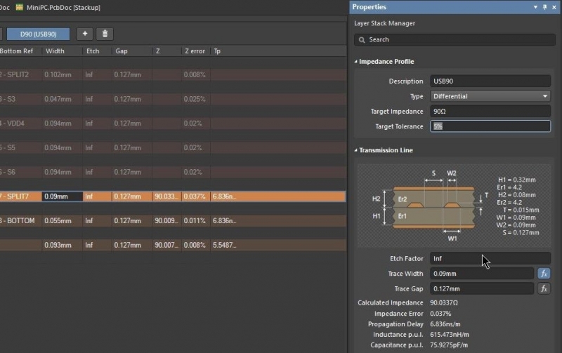
Altium Designer’s layer stack manager makes it easy to set up an impedance profile.
Layer Stackup in PCB Design with Altium Designer
When you need to create your PCB layer stackup, the layer stack manager in Altium Designer lets you specify layer types, define dielectric and core layers, and configure their order in the PCB stackup. You can also specify the board materials from Altium Designer’s stackup materials library and their thicknesses in each layer. You can also specify drill pairs, back drill information, and plan sub-layer stacks for different board regions.
PCB Stackups for Advanced Circuit Board Designs
The layer stack manager in Altium Designer is a powerful tool that allows you to interactively design your PCB layer stackup. When you’re working with more advanced PCB designs, such as flex and rigid-flex PCBs, the layer stack manager in Altium Designer allows you to define flex regions in your circuit board to connect different sections into a complete PCB. These tools are easy to use and are accessible alongside the rest of your design tools.
- PCB stackup design for advanced PCBs can be difficult without the right design features.
- Altium Designer is always being enhanced with ways to help you, like with the stackup materials library to pull materials from when building your PCB layer stackup.
Learn more about creating a PCB stackup for flex and rigid-flex PCBs.
- The CAD tools and layer stackup manager in Altium Designer make it easy to create a layer stackup for your board, including flex and rigid-flex circuit board designs.
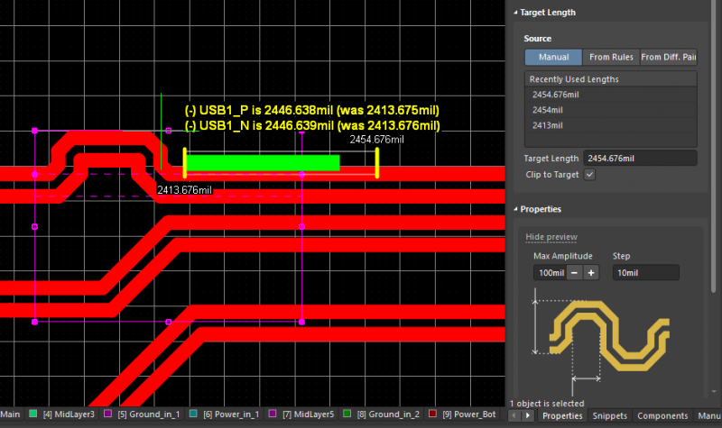
Today’s complex high-speed designs are easily handled by Altium Designer
PCB Stackup Design and Layout in Altium Designer
Altium Designer gives you the most advanced layer stackup manager so that you can control the configuration of your PCB stack up with precision. Once you’ve built your PCB stackup, you can instantly capture your schematics as an initial PCB layout. You can then route traces between components, perform signal integrity simulations, and prepare your circuit board for manufacturing. Everything you need to design your circuit board and manufacture it at scale is included in Altium Designer.
Getting your design ready for PCB fabrication involves more than just laying out your circuit board. Your fabrication documentation needs to include details like your PCB stackup, blind and buried vias, component info, and copper placement. With Altium Designer’s documentation tools, you can easily turn your PCB stackup and layout into comprehensive fabrication documentation—all in one place. No need to juggle multiple programs for design, simulations, and documentation generation. Altium Designer streamlines the entire process for you.
All the PCB Design and Layout Tools You Need
Altium Designer is the top choice for the professional PCB designer because it helps designers stay productive. You don’t need multiple tools from different vendors to design your circuit board any longer. All the design tools in Altium Designer are built to work together with seamless data exchange between different design features. This allows your routing tools to take data directly from your PCB stackup to create high-quality circuit boards.
- The core of Altium Designer is a rules-driven design engine. This unique architecture ensures your CAD tools and signal integrity tools integrate with your PCB stackup for accurate impedance calculations.
Learn more about the rules-driven design engine in Altium Designer.
- The integrated field solver in Altium Designer also takes information from your circuit board layer stackup, giving you an accurate PCB stackup calculator for impedance and propagation delay with most common trace geometries.
Learn more about Simberian’s integrated field solver in Altium Designer.
- Your routing and layout strategy starts with the right PCB stackup design for your circuit board. The layer stack manager in Altium Designer includes standard and specialty materials to build your PCB stackup, or you can specify material properties for proprietary materials.
Learn more about Altium Designer’s advanced layer stack manager.

You can create high-speed rigid-flex boards like this in Altium Designer.
When it’s up to you to design the latest circuit board with advanced technology, you don’t have to worry about how you are going to configure your PCB stackup and board layers. Altium Designer’s advanced PCB stack up tools are ideal for creating powerful new technology. Stay productive and competitive when you use Altium Designer.
Altium Designer on Altium 365 delivers an unprecedented amount of integration to the electronics industry until now relegated to the world of software development, allowing designers to work from home and reach unprecedented levels of efficiency.
We have only scratched the surface of what is possible to do with Altium Designer on Altium 365. You can check the product page for a more in-depth feature description or one of the On-Demand Webinars.


