Making the Most of Your Crystal Oscillator

In my experience, the somewhat vague information you might find in a typical crystal datasheet doesn’t enable an engineer to be wholly confident that their design expectations can be met. On the other hand, “blindly” adopting what the crystal datasheet says usually results in adequate frequency stability. If you want to get inside and uncover what is going on, you need to start thinking about the crystal as a phase-shifting network. After all, an oscillator requires the phase shift around the loop to be 360° and that this total phase shift is a precise and stable oscillation frequency.
Anyone designing a crystal oscillator will usually have “frequency stability” close to the top of their list of requirements. Hence, all the components used in the circuit (not just the crystal) must be considered with respect to the impact they may have.
This article hopes to provide insight into how a typical crystal oscillator works and then leads-on to show some of the design trade-offs needed when deciding on the best loading capacitor values and the drive resistance. We will consider the Pierce oscillator type of crystal oscillator because microprocessors almost exclusively use it. The Pierce oscillator relies on the crystal (and associated components) to produce a phase shift of 180°, which is added to the nominal 180° phase shift produced by an inverting gate.
However, we will see that the inverting gate has a significant propagation delay, which will require the crystal (in conjunction with its loading capacitors) to operate at a phase shift that is somewhat less than 180° in order to sustain oscillation. This can cause the crystal oscillator to dissipate excessive power, which is especially problematic in very low-power oscillator applications.
If you want to skip ahead to different sections, follow these table of contents links:
- Crystal Oscillator Equivalent Circuit
- Crystal Oscillator Resonance
- Impedance and Phase Shifts
- Partial Crystal Oscillator Loading
- Full Crystal Loading
- Crystal Oscillator Stability
- Recap on Loading Capacitors
- Drive Resistance and the Loaded Crystal Oscillator
- Power Consumption of the Load Crystal
- Gate Propagation Delay
- Conclusion
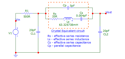
Crystal Oscillator Equivalent Circuit
For this article, I researched several different crystal data sheets and generated an approximate “average” equivalent circuit. The circuit values were fiddled-with and eventually chosen to have a series resonance set at precisely 10 MHz, which resulted in the following values:
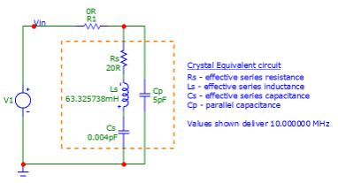
Series resonance occurs when the components Ls and Cs both have equal magnitude of impedance but, because they also have opposite impedance polarity, their effect is canceled out. This means that the orange dashed box’s left branch has, at series resonance, a net impedance of 20 Ω (Rs). So, at perfect series resonance, the above circuit’s crystal has an impedance of 20 Ω in parallel with 5 pF (Cp). Cp is also a component within the crystal and is usually specified in the datasheets.
Later on, we will show that a series resonance of precisely 10 MHz will result in an actual oscillation frequency that will be a few kHz higher. This is because Pierce oscillators cannot operate at their true series resonance (but neither can they operate at their parallel resonance). They operate somewhere between the two values, but this is nearly always closer to series than parallel resonance.
Loading capacitors were mentioned earlier, and these need to be included in a circuit model for the oscillator plus its load. From my experience, this subject area can cause confusion for a lot of engineers. We know that we need to have loading capacitors because the datasheet tells us this, and we tend to do what the datasheet says. But, do most of us really understand why they are present and what they bring to the party? Crystal data sheets also have the habit of talking about series and parallel resonance, but where does resonance fit in, and what has this got to do with the loading capacitance? So, let’s start with a theoretical examination of the equivalent circuit of a crystal.
Crystal Oscillator Resonance
If we used the well-known formula for resonant frequency (
So, the crystal (based on its equivalent circuit) at series resonance produces an impedance of 20 Ω in parallel with 5 pF. If we dug deeper, we would see that the 5 pF capacitor (Cp) at 10 MHz has a reactive impedance of 3183.1 Ω. If we crunch the numbers, this is equivalent to 19.999 Ω at an impedance phase angle of lower than 1°, i.e., still pretty close to a resistance of 20 Ω. In other words, the parallel capacitor (Cp) effect can be largely ignored in this part of the analysis.
However, this is not the frequency that the crystal will oscillate at when it’s in a typical Pierce oscillator circuit. We haven’t reached that point in the journey yet. Remember, from the discussion above, we need the crystal and its loading capacitance to produce a phase shift of 180°, and at pure series resonance, we only get a phase shift of around 1°. So, what happens if the crystal’s equivalent circuit is “tested” across a small frequency range? Below are plots of impedance magnitude (blue) and impedance phase angle (red) against frequency:
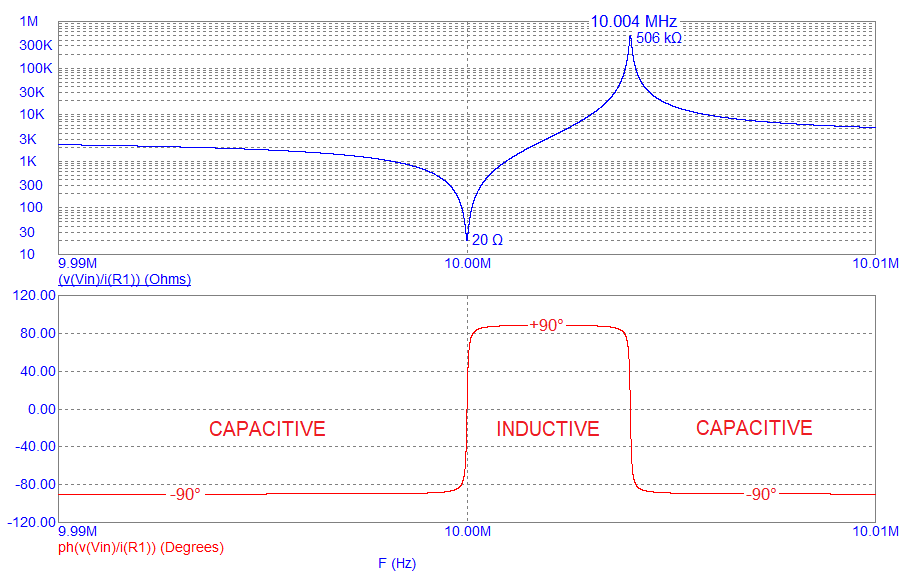
The frequency range chosen was from 9.99 MHz to 10.01 MHz and, if you look at the upper blue graph, you can see that the impedance is 20 Ω at precisely 10 MHz (series resonance). This is clearly coinciding with the value of Rs, the equivalent series resistance.
Below 10 MHz, the phase angle (in red) is pretty constant at -90°. The crystal is projecting a capacitive impedance. Immediately above 10 MHz, the phase angle has switched to +90°, and this is clearly an inductive reactance. Between 10 MHz and a little under 10.004 MHz, the impedance steadily rises towards a peak with the impedance remaining inductive at +90°.
At the impedance peak (506 kΩ), we have parallel resonance. To understand what is happening, we have to factor Cp into our thinking; the net inductive reactance formed by Ls and Cs is parallel resonated with Cp. Above 10.004 MHz, the phase shift heads back to -90°. This is capacitive impedance.
Impedance and Phase Shifts
There are two exciting areas in the above impedance plot when considering the production of a viable oscillator:
- (a) when the reactance changes rapidly from capacitive to inductive, and
- (b) at a slightly higher frequency when the reactance changes back from inductive to capacitive. Both of these two points exhibit a “strong” phase change for a small variation in frequency, and both could be suitable regions to exploit when making a stable oscillator.
However, these two points are roughly centered at an impedance angle of 0° and not 180°. But, you should be able to see that if the crystal can exhibit a rapid phase angle change over a tiny shift in frequency, it is beginning to indicate how it can be used as a stable oscillator component. You might be tempted to think that “of course everyone knows that crystals make stable oscillators” however, one of the points of this article is to teardown what makes the Pierce oscillator “tick.” Sometimes, that means justifying what might seem to be obvious.
We now need to move away from analyzing the crystal’s impedance and look at ways in which we can make it work as a component inside the Pierce oscillator. We can see that places (a) and (b) above make it viable, but we still need to arrange for it to produce a rapid phase change (of the right kind) at one specific part of the frequency spectrum. We also need the push the phase shift to be around 180°.
Partial Crystal Oscillator Loading
We are now beginning to understand that the Pierce oscillator requires the crystal (and its associated loading components) to produce a rapid phase change over a small frequency range. So, the next step is building a simple circuit around the crystal and then analyzing the resulting transfer function:
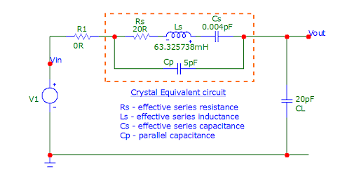
The crystal is driven from V1 (R1 set to 0 Ω) and loaded with a single capacitor of 20 pF (CL). We are interested in analyzing Vout, but we are also interested in how the phase is affected by CL:
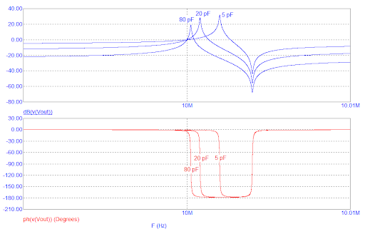
CL is varied from 5 pF to 80 pF. As you can see, this produces slightly different frequencies (above the series resonance) where the phase changes rapidly. This is demonstrating how loading capacitance can affect the stated operating frequency in the datasheet.
Below 10 MHz and just above 10.004 MHz, the phase response is 0°, and this is not a useful area for a Pierce oscillator. At just above 10 MHz, the phase angle rapidly falls to nearly 180°, but again this isn’t quite sufficient for a Pierce oscillator. From what we see in the plot above, the most viable phase angle is around -90° because the phase response is at its steepest and is the least ambiguous regarding the operating frequency. While -90° is not a very useful phase angle for an oscillator, it is a significant improvement on the “bare” crystal as its most viable phase angle was only 0°.
If we wish to make a successful Pierce oscillator, we need the phase angle to pass through 180° at one specific frequency rapidly. This is the reason why we need to use two loading capacitors located on either side of the crystal. Two capacitors will add an increased phase shift to the above responses and produce rapid phase changes that will pass through 180°.
But, to make this work, R1 cannot be zero ohms. In other words, the voltage source that would drive the extra loading capacitor has to have a non-zero resistance in order to offset the phase shift by an additional 30° or more. This leads us to the topic of full-crystal loading.
Full Crystal Loading
In this circuit, we have both CL1 and CL2 loading the crystal on either side, and R1 is now 500 Ω. Later on, we will alter R1, but for now, we’ll vary CL1 and CL2 and see how the transfer function shapes-up.
CL1 and CL2 are jointly varied from 5 pF to 30 pF in increments of 5 pF. Notice the variations in the frequency of the sustained oscillation that we would get (phase = 180°) when CL1 and CL2 vary:
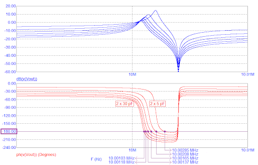
Despite these variations, the circuit is now at the stage where it is a viable Pierce oscillator circuit. We have added CL1 and CL2 to “load” the crystal, and we have recognized that in order to get a 180° phase shift, the driving source needs to be in series with a resistor (R1). This is the beginning of the end-game.
Perhaps it should also be noted that although the crystal’s equivalent circuit was designed to have a series resonance at precisely 10 MHz (within 1 Hz), the resulting (and viable) oscillator frequency might be somewhere between 10.001 MHz and 10.003 MHz.
This isn’t the type of static frequency error you will get from a real crystal that you might purchase; a real 10 MHz crystal suitable for a Pierce oscillator is designed to have its series-resonance around 1 to 3 kHz below the rated 10 MHz value. Once loaded with the capacitance specified in the datasheet, it will run very close to the specified 10.000 MHz.
It’s worth restudying the effect of the loading capacitors in the graphs above. Loading capacitance is varied from 2 x 5 pF to 2 x 30 pF and, although all the phase responses pass through 180°, when CL has a value of 2 x 5 pF, the phase angle change is less clear-cut than when using a CL of 2 x 30 pF. In other words, the slope is shallower for 2 x 5 pF, and the exact frequency where a 180° phase shift occurs is more ambiguous. The effect can be seen numerically by initially comparing the 5 pF response with the 10 pF response.
Crystal Oscillator Stability
At 5 pF, the oscillation frequency will be 10.00285 MHz, and at 10 pF, the oscillation frequency will be 10.00208 MHz. In effect, a 5 pF change in loading capacitance results in a frequency change of 77 Hz. Compare this with the frequency change when the loading changes from 25 pF to 30 pF; the oscillation frequency change is now only 15 Hz for the same magnitude of capacitance change. Therefore, increasing the load capacitance results in a more stable operating frequency.
So, to obtain better frequency stability, you should use larger value loading capacitors. However, and there’s little point in arguing about it, the crystal manufacturer will specify the correct loading capacitance and this should always be used. Still, you might be tempted to ask the following question:
- Question: Why not use even higher value loading capacitors and get better stability?
- Answer: It’s all down to the allowable power dissipation of the crystal. In other words, it’s a trade-off.
Manufacturers will typically specify the net load capacitance. If they state 10 pF, then use 2 x 20 pF capacitors because the series combination will have the required net value of 10 pF. The reason why net load capacitance is stated is because of situations where you might want to use one capacitor of 30 pF and another capacitor of 15 pF. Together, the 30 pF and 15 pF components still produce a net load capacitance of 10 pF, but there are some circuits (usually BJT oscillators) that require different values to initiate oscillation properly. With 30 pF at the driven end and only 15 pF at the crystal’s output end, there is a net improvement in the transfer gain. Regular Pierce oscillators don’t run short of gain; hence 2 x 20 pF is fine if a net load capacitance of 10 pF is stated in the datasheet.
Recap on Loading Capacitors
The crystal by itself may be series resonant at precisely 10 MHz, but for a viable oscillator circuit, we are interested in the 180° phase shift point of the transfer function. In a Pierce oscillator circuit (using an inverting gate as an amplifier), the loaded crystal circuit “provides” the extra 180° to produce an overall phase shift of 360°. Only this condition fulfills part of the Barkhausen Stability Criterion.
Some mention should also be made about the parallel resonant point and why it cannot be used in a Pierce oscillator circuit. With reference to the transfer function graph above, although parallel resonance is very unambiguous, i.e., it has a very strong change of phase over a small change in frequency; unfortunately, the transfer function amplitude has very high attenuation at this point. Oscillators that make use of parallel resonance are more specialized and are not suitable for Pierce circuit topology.
Drive Resistance and the Loaded Crystal Oscillator
Previously we fixed the drive resistance at 500 Ω and looked at the effect of varying the loading capacitors (CL). This time we’ll keep the loading capacitance at 20 pF and change the drive resistor (R1) in steps from 250 Ω to 1500 Ω:
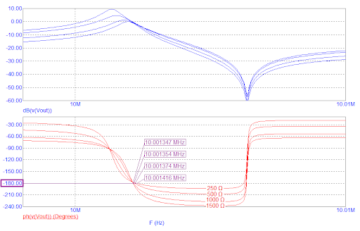
The responses all cross 180° at close to the same frequency, so the effect on the oscillation frequency is marginal compared to the impact of loading capacitance changes. However, the graphs’ steepness at the point where they cross the 180° phase shift line varies significantly. With a higher value drive resistor (R1), the frequency that produces the 180° phase shift is much less ambiguous. This means that a higher value of R1 produces a more stable oscillation frequency.
Many crystal circuits (typically those operating with 32.768 kHz crystals) have a drive resistance of many tens of kΩ. This improves frequency stability and keeps power requirements down at lower levels (ideal for battery-powered equipment).
Power Consumption of the Load Crystal
Crystal manufacturers usually specify the maximum allowable power that can be used with their devices. This maximum power is interrelated with the stated loading capacitance. Consider the current that flows in the series element Rs at the oscillation frequency. We can simulate this and plot the power dissipation in Rs (labeled pd(Rs)):
The power figures shown above are at their respective oscillation frequencies (as dictated by a phase angle of 180°). The drive level used is 2 volts peak-to-peak, feed via 500 Ω (R1).
The upshot is that if you increase the load capacitance, the crystal’s power dissipation becomes higher. More heat means a greater likelihood that the crystal accuracy is undermined. A higher drive level means more heat. So, on the one hand, you can get improved oscillation frequency stability by increasing the loading capacitance. However, the downside is that you “grow” the power dissipation significantly, which can degrade the frequency stability. Trade-offs!
Gate Propagation Delay
No matter how good the crystal is or how carefully you have chosen the component values around it, if the inverter gate has a poor performance, you will get oscillation frequency errors and possibly excessive frequency drift. Consider the 74AC04 inverter (just as an example):
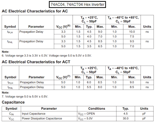
The quoted delay figures for rising and falling edges are typically around 5 ns but could be as high as 10 ns. If we take the maximum values, this means an overall output delay time of 10 ns and, because we might be designing a 10 MHz oscillator, the extra 10 ns is equivalent to adding 36° of phase shift. However, this is alleviated by the type of circuit used. For example, if we operate the gate in a semi-linear fashion, and therefore with deep saturation of the output MOSFETs, this will not occur. Still, we might expect to see a delay equivalent to something like a 20° phase shift in this arrangement.
If this happens, it means that the loaded crystal circuit only has to produce a phase displacement of 160° in order to create a viable oscillation, and this has a detrimental effect on power dissipation as we will see below:
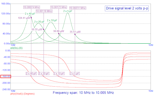
The table below summarizes all these effects. The left-hand column shows the range of loading capacitance values. The blue data taken from the graphs assume that the gate driver does not contribute any significant delay time; hence the gate delay is equivalent to 0°. By contrast, the red data assumes that the gate driver is similar to the 74AC04 and produces an equivalent delay of 20°.
|
Loading capacitance |
Gate delay ≡ 0° |
Gate delay ≡ 20° |
||
|
Required crystal shift: 180° |
Required crystal shift: 160° |
|||
|
Frequency |
Power |
Frequency |
Power |
|
|
2 x 5 pF |
10.00285 MHz |
5.35 μW |
10.00231 MHz |
35.51 μW |
|
2 x 10 pF |
10.00208 MHz |
12.12 μW |
10.00172 MHz |
38.89 μW |
|
2 x 20 pF |
10.00137 MHz |
28.73 μW |
10.00118 MHz |
56.55 μW |
|
2 x 40 pF |
10.00082 MHz |
73.88 μW |
10.00074 MHz |
104.41 μW |
We can see that the crystal power dissipation is significantly higher when the gate propagation delay is taken into account and how it affects “low-power” oscillator circuits the most. So, choose your gate carefully if you want the best stability and low power consumption.
A device specially tailored for use with crystal oscillators is the SN74LVC1404 (Oscillator Driver for Crystal Oscillator or Ceramic Resonator). It has a propagation delay (between Xin and Xout) of no more than 1.8 ns with a 5 volt supply and no more than 2.4 ns with a 3.3 volt supply. It also has an in-built gate for buffering Xout like this:

Also, note the use of resistor RF - it is needed for all Pierce oscillator circuits of the types covered. This resistor acts like the feedback resistor in an op-amp; it turns the gate into a near-linear amplifier using high-impedance negative feedback to bias the input at the “right” DC level.
I wouldn’t expect this device to produce a delay that incurred anything more than an equivalent 4° phase shift at 10 MHz. This type of chip is a good benchmark to use when comparing other potential Pierce oscillator driver gates.
Conclusion
Hopefully, you have found this article useful. The topics covered centered around using a Pierce oscillator with a crystal. Along the way, the impedance of the crystal was examined. Stage by stage, we have shown that to use a crystal effectively, it has to be part of a circuit that uses two loading capacitors and is driven via a resistor. This ensures that the circuit produces a rapid phase shift at the required oscillation frequency. We have also seen how the effect of a gate delay could worsen the crystal power dissipation and possibly take it beyond the data sheet’s limits. These delays, if temperature-dependent, might also degrade the frequency stability of the circuit.
No real circuits were harmed in the creation of this article. However, significant use has been made of simulation tools and, I would encourage anyone interested in this subject to simulate these very simple circuits. It will lead you to a much better understanding of what happens within the Pierce oscillator. The new simulation UI in Altium Designer makes it easy to set up these simulations, and you can release your design to your collaborators through the Altium 365™ platform.

About Author
Related Resources


Related Technical Documentation


Table of Contents
Take advantage of the world's
most trusted PCB design system.
One interface. One data
model. Endless possibilities.
Effortlessly collaborate with
mechanical designers.
The world's most trusted
PCB design platform
Best in class interactive
routing
View License Options
Thank you, you are now subscribed to updates.