Overlapping Planes in PCB Mixed-Signal Layouts
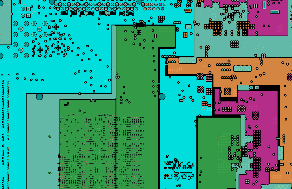
Power planes, or at least polygon pour used for power, are indispensable in modern PCBs, and it’s doubtful that digital systems as we know them would exist without the ability to split power nets into different regions. With digital boards that are nominally running at DC (possibly with some superimposed noise from a switching regulator), splitting up a power plane or using multiple power planes is a necessity for routing large currents at standard core/logic levels to digital components. But what about analog power nets and the power they provide? How do we work these into a mixed-signal PCB layout?
Once you start mixing analog and digital sections into your power layers with multiple nets, it can be difficult to implement clean power in a design if you’re not careful with your layout. At high frequencies, this can create a noticeable EMI problem up to RF frequencies when the different types of plane regions are overlapped. In this case, we need to think about how to either interleave power and ground regions in a high layer count board, or separate different power regions in low layer count boards.
The Mixed-Signal Plane Problem
One of the big debates that comes up over and over again in mixed-signal PCB layout, plane design, and stackup design is how to arrange grounds and power nets, and even what specifically qualifies as a ground. Suppose, for example, you decide to have an analog-only ground plane and a digital-only ground plane (FYI, you probably shouldn’t do this); if these plane sections are physically disconnected, which of these is defined as 0 V? Do they only share the same potential if they are connected with caps? This is not a trivial question.
The same question applies to a pair of power planes, or rather any pair of conductors separated by an insulator with a non-zero potential difference between them. If you think this sounds like a capacitor, then you’re correct! Anytime you have two planes or polygons separated from each other by the insulating dielectric, you have created a capacitor. This means the power planes will charge and discharge when a potential develops across them, including two power planes, two ground planes, or a power/ground plane pair.
Consider the arrangement of polygons below. The purple polygons are providing VDD power to two ICs, which is nominally a DC voltage; the adjacent layers are ground. The light blue region is another DC net at a different voltage being supplied by a different regulator. The question is: what would happen if we stack these in a multi-layer PCB?
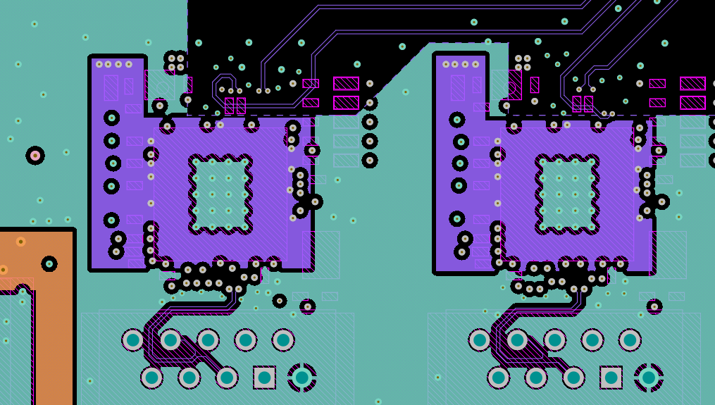
The above arrangement shows two DC nets, a situation which I’ll address in more detail later, but what if the light blue region was an analog power net? In mixed-signal PCB layouts, we have to ask the question, how should we arrange overlapping planes so that we don’t couple noise between different regions of the board? Remember that one of the main challenges in mixed-signal PCB layout is to prevent unintended interference between analog and digital signals, which will primarily degrade analog signals. Capacitance between two plane layers is problematic here, and it becomes more problematic at high frequencies.
Here’s how to better understand the effects of overlapping planes at different potentials, particularly in mixed-signal PCBs.
Overlapping DC and Analog Power
When you overlap digital and analog polygons or planes, the capacitance between the two power regions will be constantly charging and discharging as a displacement current due to the oscillation in the analog plane. This is shown conceptually below:

At high frequencies and high power, such as when power is being sourced to an RF signal via an analog power bus, this coupling between planes can create RF emissions due to the oscillating displacement current on each side of plane regions. This can be problematic in high-GHz power products, which can then excite structural resonances in the interior of the board. This then leads to strong edge emissions from the board if some suppression steps aren’t applied, such as using via stitching or more complex polygons like electromagnetic bandgap structures that would be used for antenna isolation.
Use a Single, Un-split Ground Plane
When I write “un-split”, I mean a ground plane that does not have any physically disconnected sections. It’s advisable to put analog circuits and digital circuits in different areas above the uniform ground with the idea being to take advantage of high-frequency/high-speed return paths to create some isolation. In addition, this helps to eliminate the need to route analog/digital traces back-and-forth across the board, which then reduces the number of opportunities for crosstalk. I discussed this in some detail in a recent blog post, which outlines why it’s preferable to just use a uniform ground plane.
What About Two DC Planes at Different Potentials?
When you have two power planes at different DC voltages, they will initially charge up to their respective DC voltages, and there will not be any displacement current across the planes in this steady state. However, DC planes are not really at a DC potential. Note that, because of noise from switching regulators, or transient noise due to ground/rail collapse, each plane’s potential may only be nominally DC with some superimposed switching noise in each plane. The typical noise that can couple between two DC planes is:
- Switching noise from regulators, which can span many harmonics and reach into the high MHz levels
- Noise from other sources, such as common-mode noise or any EMI received from external radiators
Below we have the preferred arrangement of power rails occupying the same layer in a PCB. This is the arrangement you might see in the top 3 layers of a 6-layer PCB where one of the layers (L3) is dedicated completely to power. As is typical in mixed-signal PCB layout, the analog components on the top layer have their own region of the PCB, so it makes sense to put any analog power in this region. Then in the digital section, we would have the DC planes running underneath these components.
The other option is shown below, where the GND and PWR layers in the above cross-sectional drawing are swapped. This now requires routing over a split in DC planes except in very precisely constructed layouts. To get around this, most designers will pour copper on the top layer so they have some ground near their traces. This approach is more appropriate in mixed signal systems that only have low speed signal outputs or configuration signals, while the preceding example is better in general.

Summary
If you tie all grounds to a single reference plane as your system ground, then any grounds you use will (or should) have the same 0 V potential definition in the system. This means the distinction between analog and digital ground is meaningless, and we only have to worry about analog and digital power.
Determining the best power and ground plane arrangements can be challenging in any PCB, including in a mixed-signal PCB layout. Use the CAD tools in Altium Designer® to define your power/ground regions and create your physical layout. When you need to evaluate signal integrity and EMI in your PCB layout, Altium Designer users can use the EDB Exporter extension to import their design into Ansys field solvers and perform a range of powerful signal integrity simulations. When you’ve finished your design, and you want to release files to your manufacturer, the Altium 365™ platform makes it easy to collaborate and share your projects.
We have only scratched the surface of what’s possible with Altium Designer on Altium 365. Start your free trial of Altium Designer + Altium 365 today.


