Sequential Lamination vs. Sub-Lamination PCB Stackup Builds

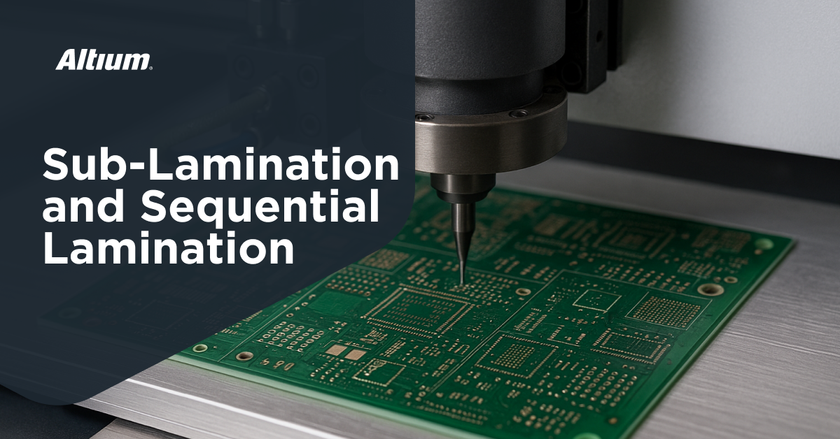
Two methods for building PCBs with blind and buried vias are sequential lamination and sub-lamination builds. The basic processes have similarities, but the order of steps and resulting board characteristics are different. Both processes are important for designing PCBs with blind/buried vias or HDI PCBs with microvias.
Due to the process used to fabricate these two kinds of PCB stackups, they impose additional DFM constraints which require understanding the overall process for building these boards. I will discuss these points for both processes in this article.
PCB Stackup Fabrication With Sub-Laminations
Sub-lamination PCB builds are fabricated by gluing multiple sub-laminations together with prepreg. A sub-lamination in a PCB stackup is a layer stack with its own set of blind and buried vias. Once these sub-stacks go through the standard via fabrication process of bonding, drilling, and plating, multiple sub-stacks are then laminated together.
The process flow below outlines the process of building sub-stacks. It is a circular process that ends once the stackup reaches its desired layer count. At the end of the process, final through-hole drilling and plating is performed.
Click on each process step below to learn more.
The stack, drill, and plate process is highly scalable and forms highly reliable vias as long as aspect ratio limits are obeyed in each sub-lamination. However, sub-lamination builds rely on mechanical through-hole drilling, as can be seen due to the typical depth of drills in a sub-stack. This prohibits two capabilities that are possible with laser-drilled microvias in sequential lamination:
- Stacked blind and buried vias are prohibited
- A via span cannot end on the same layer a different via span starts
Read this article to learn more about PCB design rules in sub-lamination builds
This limitation is imposed due to the constraints of controlled depth drilling. Those who are familiar with back drilling are likely aware of the depth tolerances in control of depth drilling. A typical depth tolerance could be anywhere from +/-2 mil to +/-10 mil; compare this to the target you would like to hit, which is approximately a 1 mil thick sheet of copper foil. If we were to try and perform controlled depth drilling in a sub-lamination, similar to sequential lamination, it is highly likely we would punch through the destination layer during drilling.
An alternative approach to implement a non-stacked blind/buried via connection, where the different spans start and end on the same layer is to use backdrill-and-fill. See the example below; in this example, a sub-lamination is formed by fabricating a buried via.
The next layer set is bonded using prepreg, and another via is formed in the outer lamination. This outer via starts as a through-hole that nests the internal buried via, but this is then backdrilled to remove the long stub while still allowing the two vias to connect with a trace. Before laminating another layer set, we could fill this backdrilled hole with an epoxy to prevent excess resin flow from the PCB dielectrics.
Sequential Lamination for HDI PCB Stackups
Sequential lamination is the process of laminating successive layers of HDI buildup film onto a stackup to create an HDI PCB stackup. Sequential lamination uses laser drilling in HDI buildup films to form blind and buried vias down to small drill diameters. It is a higher-touch, higher-precision process than standard through-hole drilling.
I have outlined the process flow in the interactive graphic below. In this process flow, we first fabricate a core layer, which may have a mechanically drilled buried via, or it may have multiple sub-laminations built using the standard process outlined below. The internal core then has the HDI layers laminated around it in the sequential lamination process.
Click on each process step below to learn more.
Sequential lamination relies on laser drilling, which also relies on thin layers in order to fabricate reliable microvias. The laser drilling process also allows different via spans to start and end on the same layer, and even allows stacking of these vias thanks to the high precision of laser drilling.
Before designing for the sequential lamination process, some important design constraints must be implemented:
- Determine the acceptable number of stacked microvias
- Select a starting copper foil thickness that will enable your etch size and clearance limits
- Ensure your target drill size complies with aspect ratio limitations, usually less than 0.75:1
- Match CTE values across dielectric layers, especially for stacked microvias
There are more specialized builds available, such as ELIC, where the entire stackup is built to control lamination and there is no buried core via region. Another design type can be used where only one side of the board is put through sequential lamination to build microvias, while the other side of the board is subject to conventional etching and drilling. All of these designs demand fabrication house collaboration to ensure producibility and reliability. Make sure a fabricator approves your PCB stackup before beginning your design.
Mixed Technology PCB Stackups
It is possible to mix these technologies such that blind and buried microvias are used alongside blind and buried mechanically drilled vias. For example, this may involve bonding HDI buildup film to a complex sub-lamination build. This would create a more complex PCB stackup that mixes these via types in different layer spans. For example, see the stackup below.
This type of build is possible because the typical buried core via region used in a sub-lamination build relies on mechanical drilling, and it is pressed into the sub-stack before bonding the HDI buildup film layers. When building the internal sub-stack, we could divide it up into multiple sub-laminations if the design requires it. Always make sure your fabrication house approves the desired stackup before starting your PCB layout.
Whether you need to build reliable power electronics or advanced digital systems, use Altium’s complete set of PCB design features and world-class CAD tools. Altium provides the world’s premier electronic product development platform, complete with the industry’s best PCB design tools and cross-disciplinary collaboration features for advanced design teams. Contact an expert at Altium today!


