


Beyond Traces: Why Soldermask May Be the Critical Factor in Ultra HDI

At a Glance
Ultra HDI success depends on more than traces. Learn why soldermask is a critical factor in manufacturability, reliability, and yield.


As PCB designers, we spend a lot of time focusing on the high-profile aspects of Ultra High Density Interconnect (UHDI) technology: tight trace widths, sub-50 micron spacing, stacked microvias, and advanced material sets. But there’s another layer that doesn’t get nearly enough attention and, in many cases, can make or break the manufacturability of your board: soldermask.
In UHDI designs, where line-and-space geometries are pushing the lower limit of what’s manufacturable, soldermask is no longer just the green coating you throw on at the end. It becomes a vital component of the electrical isolation, mechanical protection, and ultimately, the success of your layout. If your spacing is 25 microns or less, soldermask is a key design constraint.
Let’s work through why this matters, what the real-world constraints are, and how you can design with confidence as you tackle this miniaturization constraint.
The Fundamental Role of Soldermask
At its core, soldermask serves three primary functions:
- Insulates exposed copper that isn’t meant to be soldered or contacted
- Prevents solder bridging during assembly, especially in areas with high pad density
- Adds environmental and mechanical protection to outer layer copper
As the PCB moves from traditional HDI into the realm of Ultra HDI with trace widths dropping below 50 microns and copper spacing following closely behind, the tolerances for soldermask registration and resolution become incredibly tight.
Common Soldermask Challenges
One of the most common issues designers run into when moving into finer geometries is assuming that the soldermask process can keep up with the copper features. But unlike copper, which is patterned through photolithography and etching with relatively high fidelity, soldermask is screen or spray coated and then imaged. Even with laser direct imaging (LDI), there are mechanical and chemical limits to how tightly it can register.
Here are the major design pitfalls to avoid:
- Slivers: Soldermask slivers smaller than 75 microns tend to peel or lift during processing. They simply don’t have enough surface area to stay anchored. These can lead to exposed copper, potential shorts, or field failures.
- Narrow dams: Dams narrower than 100 microns are difficult to process consistently. As you reduce spacing between pads or traces, those dams become the last line of defense against solder bridging. If they’re too narrow, they may not form completely or may be compromised during assembly.
- Registration errors: While LDI can register within ±10 microns, conventional phototooling can have alignment tolerances of ±50 to 75 microns. This is approximately the sliver feature size, giving a potential error of up to 100%. If your design doesn’t allow for that tolerance, you risk mask encroaching on pads or missing coverage entirely.
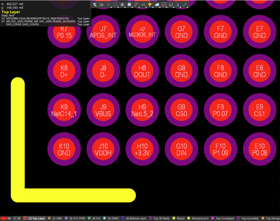
In fine-pitch packages, the soldermask expansion between pins will often leave behind small slivers, such as in the BGA footprint with 2-mil pad expansion shown below.
Design Tips for Managing Tight Spacing
What can you do to set your design up for success? Here are some practical guidelines based on today’s soldermask capabilities:
- Use mask-defined pads for spacing below 75 microns. In these designs, the soldermask aperture defines the exposed area of the pad. This allows the mask to overlap slightly onto the pad, ensuring electrical isolation even if copper features are tightly packed.
- Maintain 100-micron solder dams wherever possible. If your layout absolutely requires tighter spacing, increase the soldermask expansion (aperture) so there’s still sufficient coverage. Think of it as making the mask smarter, not tighter.
- Green soldermask. It may seem like a cosmetic choice, but it’s not. Translucent green allows for finer feature imaging than black, white, or even blue masks, which tend to absorb or scatter exposure energy unevenly. If you're pushing below 50-micron features, green will give you the highest yield.
- Avoid “just enough” spacing. For trace-to-pad and trace-to-trace distances, err on the side of giving a little extra margin where possible. If you’re relying on copper-defined pads, you’ll want at least 50 to 75 microns of spacing to allow for mask alignment tolerance and full trace coverage.
The Technology Enabling Fine-Feature Masking
Soldermask technology has come a long way in recent years. Advances in both material formulation and imaging methods have made Ultra HDI designs more manufacturable than ever before. Here are a few enablers worth noting:
- High-performance LPI (Liquid Photo Imageable) masks now use high-Tg, low-shrinkage chemistries that hold up under multiple reflow cycles and resist distortion. These resists also provide better edge definition and resist bleed, allowing for tighter clearances.
- LDI (Laser Direct Imaging) systems can achieve soldermask registration accuracy within ±5–10 microns. This precision is critical for Ultra HDI designs, where mask-to-pad alignment must be near perfect to avoid creating shorts or exposed features.
- Dry-film soldermask (DFSM) is making a comeback for very fine-feature applications, especially in IC substrate manufacturing. It offers excellent dimensional control, tight tenting over microvias, and high resistance to undercutting, which is key for dense interconnect areas.
What’s the Minimum Spacing I Can Get Away With?
This is one of the most frequent questions I hear, and the answer is: it depends on how you define your pads.
- With mask-defined pads, you can go as low as 25 microns from pad to trace or pad to pad, assuming LDI imaging and tight process control.
- With copper-defined pads, it’s safer to allow at least 50 microns, and ideally 75 microns, to accommodate mask registration and ensure full coverage.
- For inner layers, where soldermask isn’t applied, copper-to-copper spacing can be even tighter—down to 25 microns or below—depending on the etch and copper thickness.
Final Thoughts
Ultra HDI PCB design opens the door to amazing levels of performance and miniaturization, but with that comes the responsibility to design with manufacturing in mind. Soldermask isn’t just a protective coating anymore, it’s an integral part of the electrical and mechanical integrity of the board.
Take time to understand the specific soldermask capabilities of your fabrication partner. Ask about their LDI resolution limits, minimum dam widths, preferred mask colors, and whether DFSM is an option for your stackup. It’s these little details that can make or break a high-density design.
About Author
Related Resources
Related Technical Documentation
Table of Contents
Design to Release, Without the Friction
- Keep reviews tied to the right version
- Reduce handoff confusion and rework
- Spot sourcing and release risk earlier
- Work solo, share when needed
Get Started
Thank you, you are now subscribed to updates.