


High Voltage PCB Design: Creepage and Clearance Distances for High Voltage

At a Glance
Designing high voltage PCBs following specific spacing guidelines is critical. In high density circuit boards, spacing is even trickier and more important for protection.


High-voltage products can experience multiple pathways to failure, and some of these pathways become safety problems for the users of these systems. When a product is energized up to high voltage, it could have a reliability problem resulting in a slow failure over time, or a spectacular failure resulting from dielectric breakdown. No matter which failure mode you want to prevent, both categories of failure modes are addressed by enforcing two types of spacing between conductive elements: clearance and creepage.
Clearance and creepage are both limitations on conductor spacing in a PCB. The required spacing is found in industry standards such as IPC or IEC, and some of these can be determined using a simple calculator. The two main failures we want to prevent by enforcing clearance and creepage are:
- Dielectric breakdown
- Conductive anodic filamentation (CAF)
Let's jump in and examine these factors in high-voltage PCB design.

When Does Safety Require Specific Spacing Rules?
Not every PCB design has the same rigorous rules on spacing that a high-voltage PCB design needs. In general, IPC standards on power conversion devices or AC power devices start to specify clearance values for internal and external conductors when the voltage difference between conductors starts to exceed 15 V (DC or peak AC). You should set a spacing rule between these nets in your design in these cases. As the voltage difference between conductors gets larger, the required spacing (both internal and external) also becomes larger. The exact spacing requirement depends on the standard governing the end product.
Spacing is more important in high-voltage PCB design rules because a potential difference between conductive elements on a board can create an arc if the voltage between the conductors exceeds the breakdown voltage for the dielectric separating the traces. Any arc that does occur poses a significantly higher risk to both the product and your users. To help mitigate that risk, there are standards for two primary spacing measurements in your PCB design: clearance and creepage distance.
The other factor that affects reliability is CAF (and electromigration in general). Since PCBs are built on organic substrates with some salt and moisture content, high electric fields between conductors can lead to the growth of CAF via an electrochemically induced reaction. This can happen at much lower voltages than would be required to cause dielectric breakdown.
Creepage vs. Clearance
Both of these terms are used to define distances between conductors in a PCB layout and are specified in safety standards. Creepage and clearance are defined as the spacing between two neighboring conductors, although they are defined in two different ways.
What is Clearance on a PCB?
The PCB layout rules for clearance vary based on whether conductors are external or internal, what is the voltage difference between conductors, and what are the surrounding environmental conditions (altitude, and application of a conformal coating). The environmental effects are pretty significant. Most commonly, humidity changes the breakdown voltage of air and affects the likelihood of arcing. Dust is another factor since particulates that collect on the surface of the PCB can form a track over time, shortening the distance between conductors.
What is Creepage on a PCB?
Similar to clearance, creepage measures the distance between conductors on for high voltage PCB. However, instead of measuring distance in air, it measures the shortest distance along the surface of the insulation material. Board material and environment also affect creepage requirements. Moisture or particulate accumulation on the board can shorten creepage distance the same way they do for clearance.
When you have a high-density printed circuit board design, creepage can be a difficult requirement to meet. Since moving tracks is rarely the first choice, there are a couple of other tricks for increasing the surface distance in your design. Adding either a slot between tracks or a vertical barrier of insulation can significantly increase the creepage distance without changing the trace layout on the board.
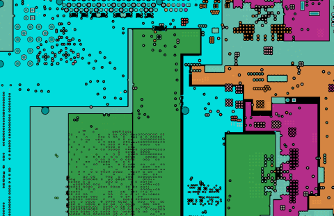
Creepage vs. clearance in a PCB. The red line shows the PCB creepage distance between two traces.
If this looks drawing a bit odd, consider the power supply PCB layout shown below. This power supply layout was modified from my flyback converter module project; in this isolated power supply, I added a slot in the region between the two sides of the transformer.
Consider pins 4 and 5 and T1; the clearance between pins 4 and 5 is the direct distance between them and will always be the same regardless of the cutout. However, the creepage distance is measured along the surface of the PCB, so it must include the bottom curvature of the board cutout in the total distance between these pins. In an isolated power supply (or any isolated system), this is a standard technique to increase creepage distance.

Consider the Comparative Tracking Index (CTI) of Your Material
After operating voltage, the most significant factor in the clearance and creepage requirements for a printed circuit board comes from the material properties of your PCB. The electrical insulation of the material is indicated by a “Comparative Tracking Index” or CTI value. The CTI is expressed as a voltage and is determined by a standardized test measuring when the surface of the material breaks down.
There are six categories from 0 to 5 based on the breakdown value of the material. The mandatory insulation levels for products are based on these CTI categories. Category 5 is the lowest, with values less than 100 V. With breakdowns of 600+ V, Category 0 has the most robust, and often expensive, material options.
In addition to the above article, the video below outlines some common characteristics of high-voltage materials.
Relevant PCB Design Standards
IPC-2221 and IPC-9592
The first important voltage-based PCB clearance standard is IPC-2221, which is the generic standard for guidance on PCB creepage and clearance. This standard is full of requirements on material quality, traceability, layout guidelines to ensure quality and much more. You can also use a high-voltage clearance calculator based on the IPC-2221 standards to determine the minimum spacing you should use for your PCB. The spacing standard is delineated by the following:
- Internal vs. external conductors
- Presence of a conformal coating (such as a solder mask)
- Altitude
- Component lead vs. copper pad
A related standard that applies to power converters for IT and computer equipment is IPC-9592. The standard specifies a voltage-based spacing requirement that is more conservative than IPC-2221, especially for high-voltage lines on internal layers. The standard does not distinguish between internal and external layers, altitude, or the presence of a conformal coating. IPC-9592 defines "power conversion devices" as any AC/DC or DC/DC module, converter, or PCBA with applied voltage differences between conductors below 500 V (DC or peak AC).
We have created simple calculator applications which can help you determine the relevant spacing requirement under these two standards.
IEC-60950-1 (2nd edition)
The second important standard is IEC-60950-1 (2nd edition). The IEC version is the standard you want to read for any IT products with AC mains or a battery power supply, especially if you want to sell those products internationally. These standards specify safety requirements on everything from office shredders to telecommunications equipment.
Because the consequences of incorrect spacing vary from legal non-compliance to serious injury and destruction of important equipment, it’s well worth the time to become acquainted with any standards that are relevant to your design. Plus, it keeps the undergrads from zapping themselves.
Additional Standards For High Power: IPC-2221 Trace Heating and IPC-2152
Many designs running at elevated voltage could also run at high currents. For example, automotive motor inverters, utility-level power management systems, and industrial systems require high power delivery to a load, requiring both high voltage and high current design approaches. Another example is DC/DC converters, which may run at high voltage in one area of the design but high current in another area of the design. These products follow additional standards which were developed to address thermal management requirements: the IPC-2221 thermal standard and IPC-2152.
The IPC-2221 standard also provides a method for sizing traces to keep average temperature at a specified limit, assuming the current in the trace is running at DC. To speed up the usage of this standard, we have created a calculator for this calculation, which can be accessed for free in the blog linked below:
While the IPC-2221 trace heating calculation is simple, it is widely known to be very conservative when used with heavy copper and nearby planes/coplanar ground. This leads to usage of very large traces or rails, and possibly plane layers, when they are not needed simply due to fears of excess heating in the design.
For these reasons, the IPC-2152 standard was developed to provide more accurate PCB design guidance in complex multilayer boards. The calculation is more complex, but a closed form result in the standard can be used to develop a calculator for determining copper rail area and width for a given temperature rise target. The calculator can be accessed below, and the video below a longer overview of the IPC thermal standards related to high current design.
The CAD tools and routing features in Altium Develop are built on a unified rules-driven design engine that automatically checks your layout as you create your board. After you've figured out your clearance requirements with an IPC-2221 calculator, you can program your clearances into your design rules to ensure your board remains safe and functional at high voltage. You’ll also have access to a full set of documentation features that help you prepare for manufacturing and assembly.
Whether you need to build reliable power electronics or advanced digital systems, Altium Develop unites every discipline into one collaborative force. Free from silos. Free from limits. It’s where engineers, designers, and innovators work as one to co-create without constraints. Experience Altium Develop today!

About Author
Related Resources
Related Technical Documentation
Table of Contents
- When Does Safety Require Specific Spacing Rules?
- Creepage vs. Clearance
- What is Clearance on a PCB?
- What is Creepage on a PCB?
- Consider the Comparative Tracking Index (CTI) of Your Material
- Relevant PCB Design Standards
- IPC-2221 and IPC-9592
- IEC-60950-1 (2nd edition)
- Additional Standards For High Power: IPC-2221 Trace Heating and IPC-2152
Design to Release, Without the Friction
- Keep reviews tied to the right version
- Reduce handoff confusion and rework
- Spot sourcing and release risk earlier
- Work solo, share when needed
Get Started
Thank you, you are now subscribed to updates.

