Skip to main content
Mobile menu
PCB Design
Altium Designer
World’s Most Popular PCB Design Software
CircuitStudio
Entry Level, Professional PCB Design Tool
CircuitMaker
Free PCB design for makers, open source and non-profits
Why Switch to Altium
See why and how to switch to Altium from other PCB design tools
Solutions
For Enterprise
The Last Mile of Digital Transformation
For Parts and Data
Extensive, Easy-to-Use Search Engine for Electronic Parts
Altium 365
Resources & Support
Explore Products
Free Trials
Downloads
Extensions
Free Altium 365 Tools
Online PCB Viewer
Resources & Support
Altium / Renesas Scheme: Information for Shareholders
All Resources
Support Center
Documentation
Altium Community
Forum
Bug Crunch
Ideas
Education Programs
Professional Training / Certification
University / College Educators
University / College Students
Webinars
Store
Search Open
Search
Search Close
Sign In
PCB Design Engineers
Main menu
Home
PCB Design
Collaboration
Component Creation
Data Management
Design Outputs
ECAD/MCAD
HDI Design
High Speed Design
Multi-Board
PCB Layout
PCB Routing
PCB Supply Chain
Power Integrity
RF Design
Rigid Flex
Schematic Capture
Signal Integrity
Simulation
Software
Altium 365
Altium Designer
Enterprise Solutions
PDN Analyzer
Upverter
Education
Programs
Altium Academy
Engineering News
Guide Books
Newsletters
Podcasts
Projects
Training Courses
Webinars
Whitepapers
FREE TRIALS
PCB Design Engineers
What is Propagation Delay in High Speed PCB Design?
In high speed design you may be dealing with the question of what is propagation delay. Altium Designer gives you the design tools to expertly work with this.
Read Article
Online PCB Design Review with Altium 365
You can design a PCB any way you like, but if it doesn’t pass a PCB design review and manufacturability checks, then it will never become a real board. A PCB design review is about more than just checking DRCs, it’s about designing to satisfy your manufacturer’s capabilities and processes. PCB design reviews also give the design team a chance to examine manufacturing files and deliverables for any errors before sending data in for fabrication and
Read Article
31:31
Transmission Line Impedance Calculation With Altium Designer
Today’s PCBs contain many transmission lines. Combine this with increased clock frequencies and data rates and the result is a critical challenge to high-speed design. Neglecting these dynamics can undermine product development by compromising performance, power consumption, EMC/EMI compliance, and more - leading to delayed design cycles and opening gaps that can be exploited by your competition. Hone your high-speed design skills by joining us as we discuss the typical transmission lines encountered in today’s designs, the PCB variables that affect impedance, as well as how to create, calculate, and design transmission lines in Altium Designer. Learn how to maximize the built in SIMBEOR® engine by Simberian to craft impedance profiles and manage transmission lines in your designs. This Live Webinar recording covers the following: Current trends in electronics development PCB transmission line model and impedance calculations Transmission line with specified impedance in Altium Designer Don’t pass up on this opportunity to experience the industry’s best in class design experience!
Watch Video
Never Cross a Ground Plane Gap in High Speed PCB Design
I often browse electronics and PCB forums, and I see the same question asked over and over: Why shouldn’t I route a trace over a split in my ground plane? This question gets asked by everyone from makers to professional designers who are just dipping their toes into high speed PCB design. For the professional signal integrity engineer, the answer should be obvious. Whether you’re a long-time PCB layout engineer or a casual designer, it helps to
Read Article
Comparing Static and Dynamic Flex Design: Rigid Flex PCB Bend Radius and other Mechanical Considerations
Static and dynamic flex PCB design is as much mechanical as it is electrical. Here are some design tips for both types of PCBs.
Read Article
Impedance Controlled Routing for Boards Made in Altium Designer
The 3D field solver in Altium Designer makes impedance controlled routing easy and lets you create design rules for your system.
Read Article
Get to Know Microvia Manufacturing Processes and HDI Substrates
Initial HDI Fabrication High Density Interconnect printed circuits actually started in 1980, when researchers started investigating ways to reduce the size of vias. The first innovator is not known, but some of the earliest pioneers include Larry Burgess of MicroPak Laboratories (developer of LaserVia), Dr. Charles Bauer at Tektronix (who produced photodielectric vias), [1] and Dr. Walter Schmidt at Contraves (who developed plasma-etched vias)
Read Article
Fly-by Topology Routing for DDR3 and DDR4 Memory
Banner image credit: Nine Dot Connects Take a look at your RAM chips the next time you're upgrading your desktop or laptop. If you need to, get the chip under a magnifying glass. Any traces you might see on the surface layer are just the beginning of a complicated web of traces between the edge connector and the RAM chips. Although the routing can get quite complicated, you can see a relatively simple topology when you take a 30,000 foot view of
Read Article
PCB Impedance Calculation and Cross Section Features in PCB Layout
When I first started laying out printed circuit boards, there wasn’t a lot of concern about controlled impedance routing. At that time, most everything was low speed and we were using larger traces and thru-hole vias for the simple four layer boards. That all changes once a board grows in speed, and changes demanded that we become more involved with the layer stackup design and specifying trace widths. At first we relied on board constraint
Read Article
Termination Methods in High Speed and High Frequency PCBs
The topic of termination will inevitably come up when dealing with high-speed digital systems. Most digital systems have at least one standardized high-speed interface, or possibly fast GPIOs that produce fast edge rate signals. Advanced systems will have many standardized interfaces which also have termination applied, normally on the semiconductor die. If you determine that you actually need termination, what method should be used? As it turns
Read Article
Crosstalk in Mixed-Signal PCB Traces and Ground Planes
Learn how to suppress mixed signal crosstalk and EMI in PCBs with the right ground and power plane arrangement.
Read Article
Build High Density Interconnect PCBs with Skip Vias
All high-density PCBs rely on specific via styles to make connections into the inner layers without taking up space for routing. This is always driven by the components used in the PCB, namely fine-pitch BGAs with many high pin counts. One of the options for routing into inner layers as part of fanout routing is to use skip vias. Type-I HDI stackups will include skip vias as part of their routing options in an attempt to avoid the use of buried
Read Article
Creating Multiple-Part Symbols for a PCB in Altium Designer
How to create multi-part components and symbols in Altium Designer
®
. Build a symbol manually or use an advanced symbol generator to do the heavy lifting of symbol creation for you.
Read Article
How to Create Schematic Symbols in Altium Designer
A step by step walk through of the Schematic Symbol Generation Tool in Altium Designer.
Read Article
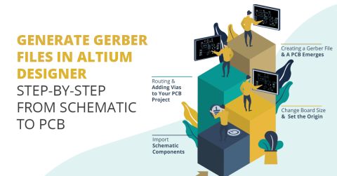
How to Make PCB Gerber Files in Altium Designer Step-by-Step
Looking for the best approach for CAM jobs? Learn how to make PCB Gerber files in Altium Designer from your circuit board layout. Altium's CAM tools can help you quickly create PCB Gerber files.
Read Article
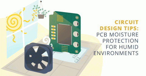
Circuit Design Tips: PCB Moisture Protection for Humid Environments
Learn more about implementing PCB moisture protection and storage in your design to prevent corrosion and board failure.
Read Article
Are Fiducial Marker Placements on PCBs Still Necessary with Modern Manufacturing Capabilities?
In PCB design, a fiducial marker is a rounded shape of copper that acts as a reference point for pick and place assembly machines. Fiducial PCB markers help machines recognize the orientation of the PCB as it passes through SMT. Based on the PCB orientation and the prior orientation of components on reels, the machine can be programmed to rotate components by specific amounts to ensure accurate placement on their land patterns. Placement of
Read Article
Pagination
First page
« First
Previous page
‹‹
Page
3
Page
4
Page
5
Page
6
Current page
7
Page
8
Next page
Next ›
Load More