






Ground Plane Connectivity in HDI PCBs Maintains Signal Integrity

At a Glance
One of the big challenges in high-speed HDI designs is ensuring you maintain enough ground connectivity. See why ground connectivity is so important in these designs in this article.


High speed PCB designs require ground connectivity across the PCB stackup. The most common way this is done in the standard stackup with lower speed signals is to use stitching vias. These vias connect multiple ground planes and pours in the PCB stackup for purposes of maintaining a clear 0 V reference everywhere along a low speed or high speed routing path.
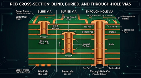
But what happens in an HDI design where vertical routing space is at a premium? In HDI designs, we often prefer to use (or need to use) blind and buried microvias to make connections for signals, and the same tendency tends to occur for ground connections. This can create major problems for ground connectivity as high speed signals move around the layer stack.
Unfortunately, there is no good way to check for the type of ground connectivity we need in HDI designs using your design rules and constraints. One reason this occurs, as we shall see, is due to pinout designs on BGA packages. I'll outline why this creates signal integrity problems and what you can do to solve it in this article.
What Creates Bad Ground Connectivity
The issue with bad ground connectivity results from the use of blind and buried vias in fanout routing, specifically on ground pins in the BGA fanout routing. The package pinout, the vias used in fanout may terminate on a layer that is not deep enough in the stackup.
The image below shows an example of good ground connectivity for a stripline route coming out of a BGA. In this example, the outer GND via terminates on a GND layer above the signal layer. The GND pin on the inner row then turns on the layer below the stripline signal. Because the inner GND via touches both the upper and lower GND planes, it helps ensure that the plane layers maintain the same 0 V reference around the stripline signal.
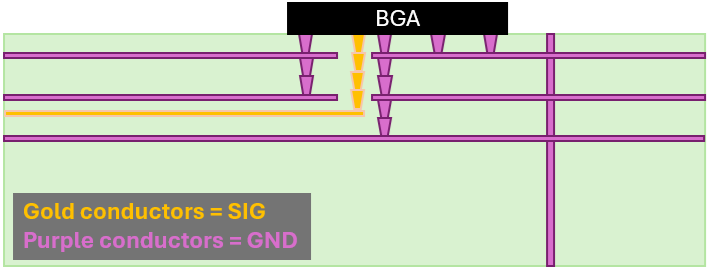
Ideal ground connectivity in an HDI design: stitching vias can run alongside signal vias to ensure a 0 V reference is maintained along the route.
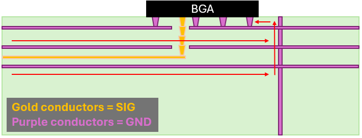
The resulting return current in this situation is traced out using arrows. The return forms the electromagnetic boundary condition for the electromagnetic field and defines the inductance along that current path. Processor pinouts are sometimes structured such that the grounds are not nicely arranged around signals, and so the automated fanout cannot create a situation like that shown above.
In some cases, a designer may think they only need one via from L1 to L2 in order to touch the first GND plane on the inner layer. The result is that return current forms around a via that is much farther from the signal being routed, especially with stripline routing deeper in the inner layers.
What exactly is the problem with this? It contributes to two signal integrity problems:
- Local crosstalk by the signal
- Simultaneous switching noise on other IOs
- Potential to measure higher radiated emissions
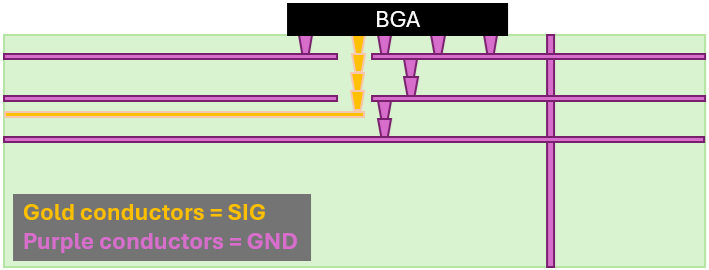
The solution is not optimal, but it is simple: place a stitching via right alongside signal transitions. In an HDI design, it's preferable to place a through-hole to help ensure all planes are at the same 0 V potential. However, BGA ball pitch may prohibit this in fanout routing. Therefore, it I'd often the case that we can only provide a blind/buried stitching via to connect grounds. In BGA fan out routing, this is actually preferable because the closest through hole via may not be accessible until you are far from the fan out region.
Sometimes, Package Pinouts Are Horrible
There is one fact that we may not like to admit, but it is certainly true: some package pinouts are absolutely horrible for ensuring ground connectivity, and this is not exclusive to HDI designs. The package designer probably views the ground pins only as the path where current leaves the chip. They are much more than that: ground pins with a stable 0 V reference form a boundary condition for the electromagnetic field. This is why, at progressively higher frequencies, Ground pins heavily influence crosstalk, via impedance matching, and insertion loss in the BGA fan out routing region.
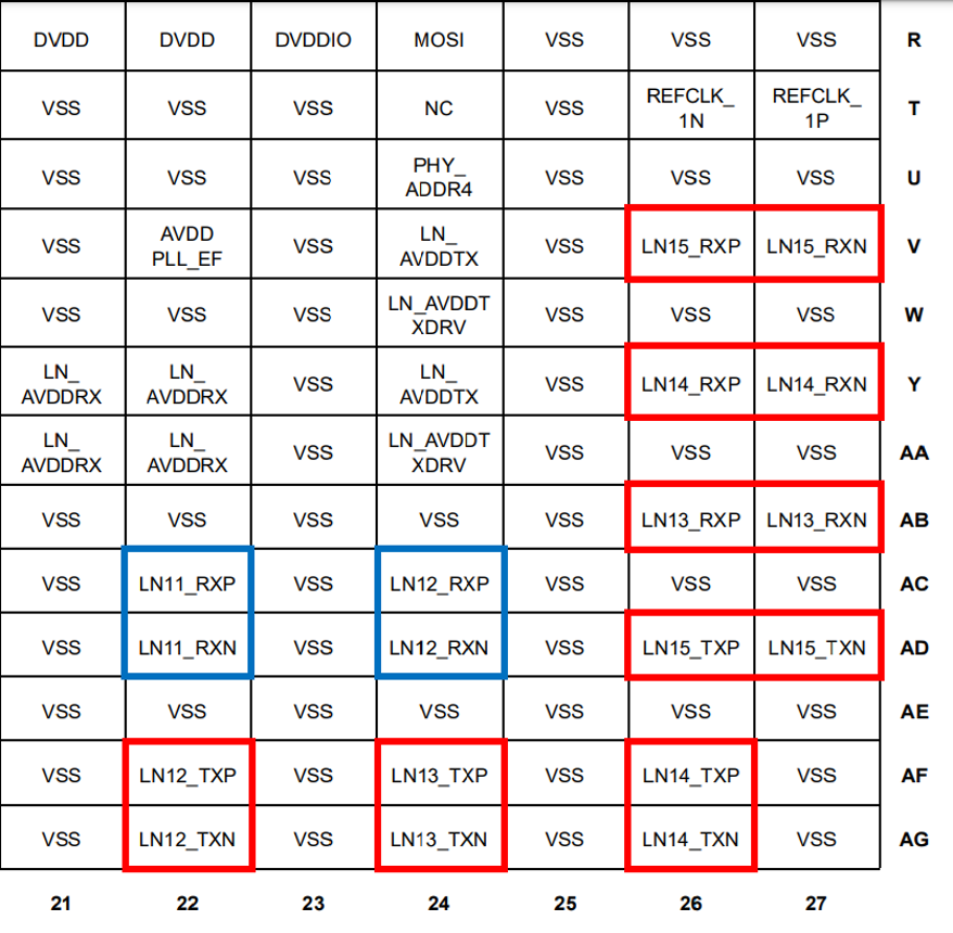
The image below shows that theoretically ideal pinout for any BGA. This is not a contrived example, it is a real pinout for Optical phy chip operating at 56G data rates (28 GHz channel bandwidth) with 0.8 mm pitch. Designs operating at higher data rates (112G-PAM4 and 224G-PAM4) push as low as 0.5mm pitch as this is required to maintain a low-dispersion transition for high-speed serial signals.
56G-phy-ballout.png
At 0.8mm pitch and high layer counts, the PCB will almost always be too thick to use through-hole vias for fanout routing due to limitations on high aspect ratio vias. Therefore, we typically stack microvias and stagger over to buried vias to reach the inner signal layers. In the above example, the ground vias placed next to the signal vias always ensures that ground connectivity can be maintained for stripline routes; each signal row will have a dedicated ground row behind it that connects to both planes.
Example 1: NRF54LM20A-PAAA
Now let’s look at some real pinouts for HDI designs. The image below shows a routing example for part number NRF54LM20A-PAAA from Nordic Semiconductor. The ground pins are indicated with yellow outlines. Although this is a 98-pin fine-pitch BGA (0.35 mm pitch), it only has 11 ground pins sparsely spread around the pinout.
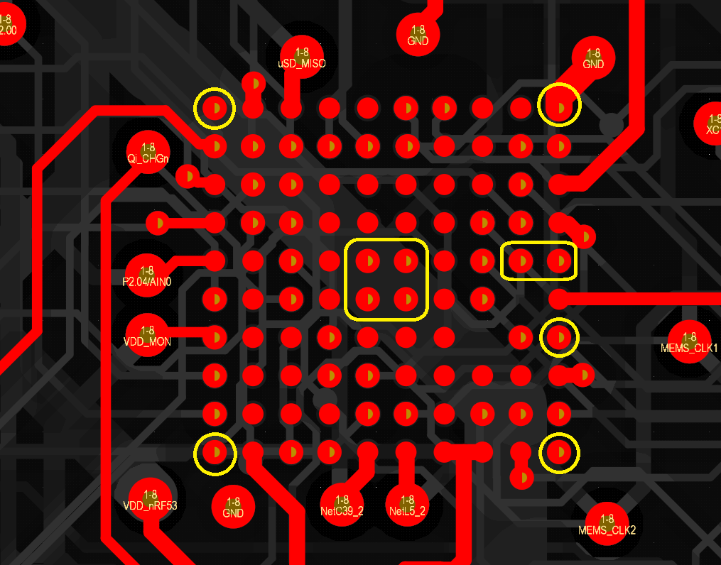
Location of GND balls in an NRF54LM20A-PAAA package. The small pitch (0.35mm) prevents the use of standard through-hole vias.
Although the design contains some GND pins which are close to many of the signals, they are only directly connected to the ground plane on L2 with blind microvias. There are 3 nearby through-hole GND vias, but these are the only vias that connect to internal planes near the microvia signal transitions in the BGA fanout region.
That would put this device at risk of ground bounce noise and crosstalk in the fanout routing area; however, given the high supply voltage allowance and thus the large noise margins on this component, it may not be much of an issue. But when we look at another type of component, such as high-speed memory, we can see why this can be a major problem. Ideally, we would need to complete two tasks:
- Add in more GND through-holes around the edge of the BGA
- Include internal stitching vias when transitioning signals are far from through-holes
Of course, whether or not this is really a major problem depends on the signals in question, particularly where EMI from via transitions is concerned. The fastest interfaces on this component are the USB interface and SPI lines; the latter will be the interface with the greatest EMC risk (for reasons I discuss here). With that being the case, the SPI lines need the closest stitching vias, while loaded down GPIOs or I2C lines can often get away without closely located stitching vias.
Example 2: Custom DRAM Module
Now let’s look at another pinout for a custom DRAM module (DDR4-3200 memory) from a major semiconductor vendor. This particular module is popular in embedded computing systems and it aggregates high bytelane count into a single module. The footprint is shown below with the GND pins highlighted.
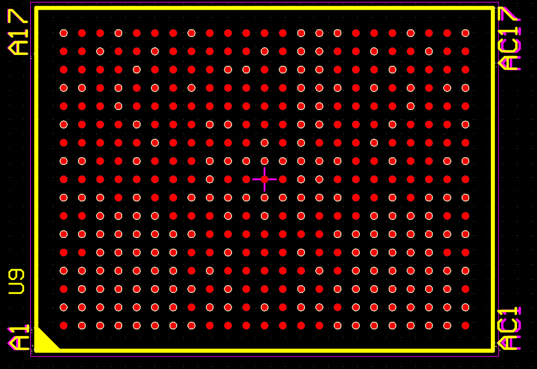
Custom DRAM module footprint. The highlighted pads show the ground pin.
If you use L1-L2 blind vias for the ground pin connections, you will be guaranteed to see simultaneous switching noise and high crosstalk in the fanout region. Any signal that routes into an inner signal layer (L3, L5, etc.) will have no nearby stitching via connection if only L1-L2 blind vias are used for the ground pins.
Because this component is designed in a non-JEDEC package and it does not include the standard routing channel, it requires at least 4 or 5 signal layers to solve the routing (point-to-point). In addition, the arrangement of signal pins will require stacked microvias and a buried via to reach all the signal layers. However, it should be clear that the location of grounds in the pinout causes some signals to be located far from a ground pin.
Solving this problem requires:
- Planning a blind/buried via transition on all the GND pins to connect all GND planes below the module
- Placing additional through-holes around the package boundary
- Placing internal buried microvias/buried mechanical vias for layer-to-layer stitching
Now compare this to the typical JEDEC-standardized package for a DDR memory, such as the DDR4 memory chip from Micron shown below.
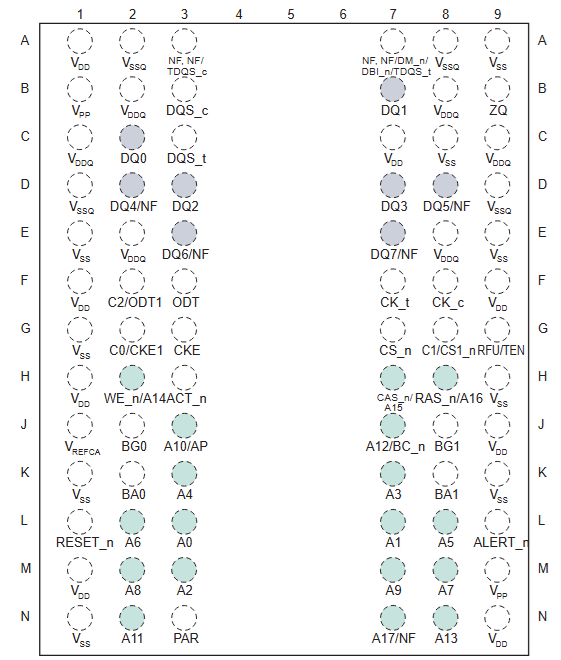
Why is this package more likely to have better performance in terms of ground bounce, crosstalk, and EMI?
- The pin count and row/column count is lower, so it’s likely the layer count will be low enough to allow through-holes.
- The pitch is 0.8mm, which is large enough to allow through-holes in dog-bone fanout or via-in-pad.
- Almost all the high-speed signal pins are no farther than 1.6mm (2-pin distance) away from a VSS pin.
- The routing channel allows for some additional stitching vias as needed, for example in the A7/A9/A13/A17 region.
If the custom module pinout were being used for only a component with slow-speed signals, then the design would likely not be problematic in terms of crosstalk, ground bounce, and EMI. However, this component contains multiple DDR4 interfaces clocked at 1600 MHz (3200 MT/s data rate), which requires a fast edge rate for timing purposes. That much faster edge rate makes the SI, EMI, and crosstalk problems associated with insufficient GND connections on internal signal layers much more noticeable.
The Solution: Place the GND Vias First!
The greatest mistake a designer can make in these designs is to place the vias for the GND pins after routing the signal pins. If you place the GND vias first, they will act as routing constraints against your signals and you’ll be forced to route around them, but you avoid an important set of SI problems in an HDI design. This is highly preferable to routing everything in an HDI design, then realizing you did not include enough ground vias in the fanout!
Whether you need to build reliable power electronics or advanced digital systems, use Altium’s complete set of PCB design features and world-class CAD tools. Altium provides the world’s premier electronic product development platform, complete with the industry’s best PCB design tools and cross-disciplinary collaboration features for advanced design teams. Contact an expert at Altium today!

About Author
Related Resources
Related Technical Documentation
Table of Contents
Solutions for Every Role and Team
- Discover and evaluate design options earlier
- Develop in one shared workspace
- Scale with control and compliance
- Connect every stage of hardware development
Learn More
Thank you, you are now subscribed to updates.



