




How Does Copper Weight Affect Signal Integrity in UHDI PCBs?


I have talked about the reasons why smaller line widths and smaller clearances require lower copper weight in videos and articles. The primary reason is that manufacturers cannot etch copper down to very small trace width and spacing, such as 2 mil/50 micron values, when the base copper foil becomes similar to the copper track width. For this reason, the smallest line widths and spacings used in HDI PCBs tend to exhibit traces that have something closer to a square aspect ratio rather than a wide trapezoid. This is especially the case in stripline layers.
With thinner copper films correlating to thinner line widths, what happens to the line impedance? And in particular, how will the line impedance vary for a given variation in the copper thickness? These are important questions because they will influence the amount of margin you can accept in a simulation of a transmission line, antenna, printed RF circuit, or any other circuitry that requires copper to maintain impedance control. I will examine these points in this article, as well as show some data on line impedance variations given real variances in copper film thickness.
What Copper Looks Like in UHDI
As was mentioned above, copper traces in a UHDI design have something closer to a square cross section rather than a typical rectangular or trapezoidal cross section. Subtractive etching is responsible for creating the trapezoidal cross section; this is because etchant continues to eat away on the exposed surface of copper foil. As copper weight reduces, the etching time is lower, and this reduces the etch factor on a trace, making it look more square.
The typical dividing line between HDI and UHDI is where we need to use additive processes; SAP or mSAP is needed to fabricate linewidths below 50 microns used in UHDI designs. With an additive process, there is no etching and the deposited copper will look much more square than etched copper. The image below shows an example of additively deposited traces on Ajinomoto buildup film (ABF) as striplines. The traces are deposited on ABF and then covered with a bonding layer to form the striplines.
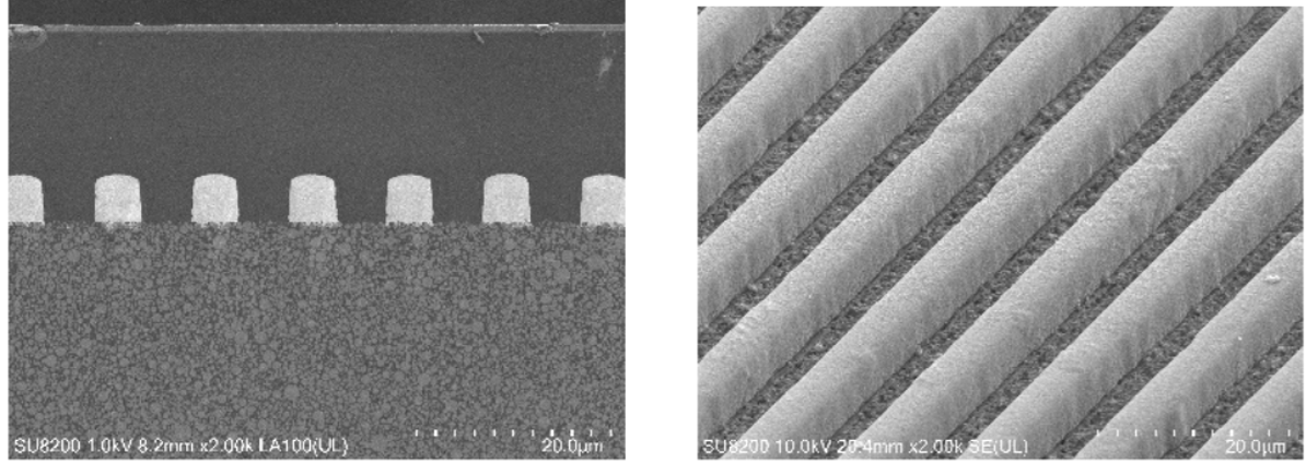
The amount of variation in these traces is quite small, only a few microns across the traces shown in the left image. Compare this to the cross section dimensions, which are approximately 40 microns horizontal and vertical. Compare this variation to a typical etched trace, where roughness alone can account for a few microns, and edge uniformity and foil planarity can produce similar variance.
In regards to signal integrity, this raises two important questions:
- How do copper thickness variations impact impedance?
- How do these impacts compare at standard copper weight values versus film thicknesses in UHDI?
Studying the Impact on Impedance at Large and Small Copper Weights
First, let's consider what happens in typical standard PCB builds. Base copper weight is typically 0.5 oz per square foot base foil, and the outer layers are plated up to approximately 1.0 oz per square foot copper thickness in order to fabricate the through hole vias.
In an HDI design produced with subtractive etching, base copper weight could start at 0.25 oz per square foot in order to allow for smaller line widths and clearances. Holes can then be selectively plated so that proper weight is not impacted during microvia fabrication, and the outer layers may be cleaned up to between 0.5 oz per square foot and 1.0 oz per square foot. In additively fabricated UHDI PCBs, copper weight could be as low as 1/8 oz per square foot.
PCB Build Type | Copper Weight |
Standard build (base foil) | 0.5 oz/sq. ft., plated up to ~1.0 oz/sq. ft. on outer layers |
HDI (subtractive etching) | 0.25 oz/sq. ft. base, outer layers cleaned up to 0.5–1.0 oz/sq. ft. |
UHDI (additive) | As low as 1/8 oz/sq. ft. |
We can use the Layer Stack Manager in Altium Designer to calculate changes in impedance while varying the copper weight around these values while keeping the same trace width. This allows us to extract a curve showing the impedance changes as the copper weight changes due to natural process variations.
Results
After running multiple simulations holding trace width constant and changing the copper weight, the curves shown below were extracted for striplines and microstrips targeting a 50 Ohm impedance. These curves show a general downward slope in the impedance as copper slightly increases, which follows our intuition about trace impedance. However, the interpolated data and its derivative indicate that the trace impedance changes are greater when the starting copper film thickness is smaller.
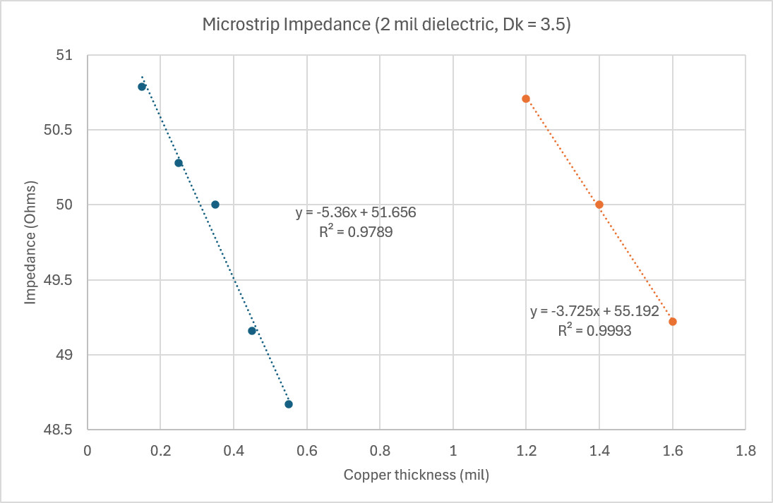
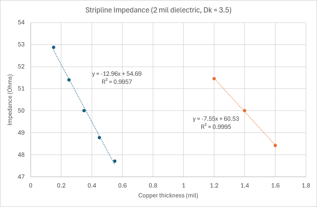
Now compare these thickness changes in the graph above to the thickness changes seen in the SEM image of the striplines on ABF. Just due to a few microns variation in the additive deposition process, we could expect 1.5–2 Ohms variation in trace impedance for a 50 Ohm stripline. If you have a standard 10% tolerance value for the trace impedance, that equates to about 30–40% of your allowed margin already eaten up by process variations.
What about a subtractively etched board? The same variation (a few microns) is typical of what we would see in the roughened copper for striplines. The graphs show a smaller impedance variation (about 50%). However, here the impact is more important in terms of loss from increased skin effect, which produces its own impedance variation at high frequencies.
What It All Means for Signal Integrity
The result above for the additively fabricated UHDI board means that, in reality, your fabricated PCB only has a 6–7% impedance tolerance allowance, not 10%.
A few percentage points might sound small, so how does this impact signal integrity? It essentially requires you to increase the allowed margin you would accept in an S-parameter plot for determining channel bandwidth. There is a de facto -10 dB S11 limit above which we generally consider the impedance to be too far away from its target. This will require you to apply additional margin, possibly setting the maximum loss value to as low as -15 dB to ensure sufficient margin.
In high-bandwidth serial channels or in dense parallel channels that experience a lot of crosstalk, every little bit of noise margin matters, and that is where the losses are observed in a measurement or eye diagram simulation. There are still not sufficient design approaches to account for this variance other than to look at the potential range of variation in S-parameters, which can be simulated or measured on test coupons.
Whether you need to build reliable power electronics or advanced digital systems, use Altium’s complete set of PCB design features and world-class CAD tools. Altium provides the world’s premier electronic product development platform, complete with the industry’s best PCB design tools and cross-disciplinary collaboration features for advanced design teams. Contact an expert at Altium today!

About Author
Related Resources
Related Technical Documentation
Table of Contents
Solutions for Every Role and Team
- Discover and evaluate design options earlier
- Develop in one shared workspace
- Scale with control and compliance
- Connect every stage of hardware development
Learn More
Thank you, you are now subscribed to updates.



