








Optimize Performance and Design Flexibility with Structural Electronics


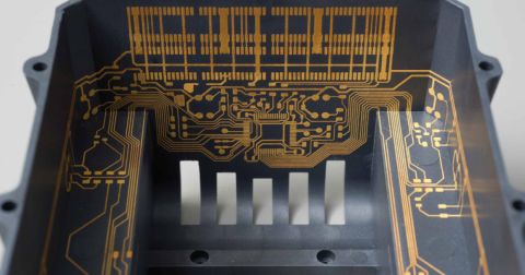
When the product enclosure becomes the circuit board, the design rules change entirely. Structural electronics, built on technologies like 3D molded interconnect devices (3D-MIDs), embed conductive traces directly onto molded plastic housings, eliminating the separation between the electrical and mechanical worlds.
That integration is the point. It enables smaller footprints, better thermal management, and native EMI shielding. It also means that a single mechanical geometry change can destroy an electrical trace. This illustrates another instance where electrical and mechanical engineers need to collaborate on innovative designs, with live data sharing throughout the process.
Key Takeaways
- Structural electronics merge the enclosure and circuit board into one, embedding conductive traces directly onto molded plastic housings to enable smaller footprints, better thermal management, and native EMI shielding.
- A single mechanical change can break an electrical design. Structural substrates replace standard PCB materials, creating new tradeoffs around thermal dissipation, signal integrity, and shielding durability that both EEs and MEs must account for.
- Component and package selection must adapt to 3D manufacturing constraints. Z-axis limitations, extreme heat and pressure during molding, and surface curvature all restrict which IC packages and materials can be reliably used.
- Structural electronics require live, cross-discipline collaboration throughout the design process. Static file handoffs between electrical and mechanical teams create unacceptable risk when a geometry change can destroy a trace.
Structural Electronics Demands Hardware Collaboration
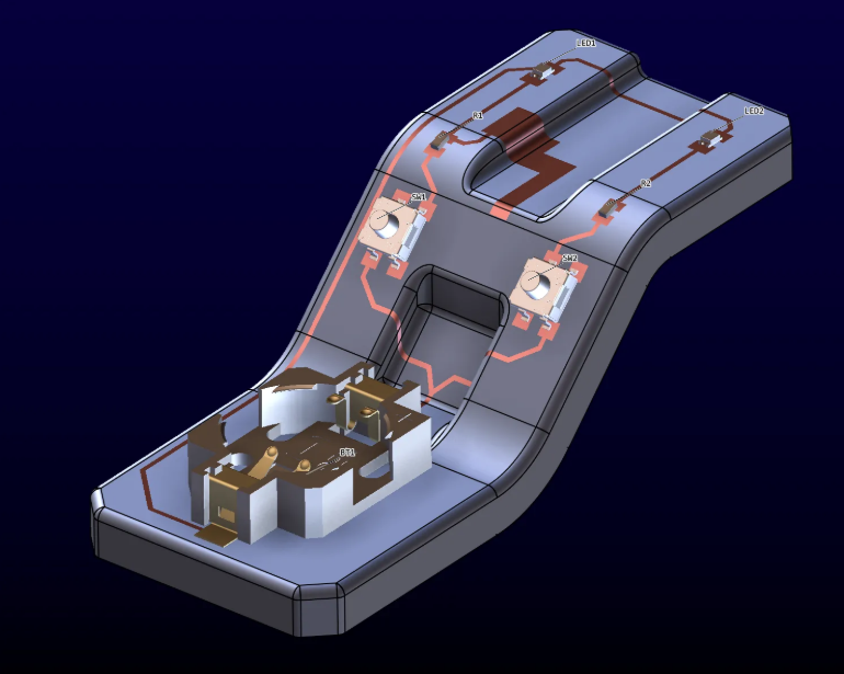
Pivoting to structural electronics removes traditional design boundaries. By utilizing an appropriate 3D CAD software and designing for a 3D deposition process, engineers can discard the limitations of flat, rigid boards and route conductive traces along any 3D molded plastic surface.
Structural electronics enable unique solutions to engineering problems involving thermal management, high-speed and RF design, and even electromagnetic interference (EMI). Because the substrate itself becomes a fully integrated component in the design, a different set of tradeoffs arises as standard PCB materials are no longer used.
Thermal Dissipation
- Chassis-level heatsinking: Transforms the outer housing into a giant, distributed heatsink, conducting thermal energy directly to the exterior surface area.
- Complex 3D placement: Forces engineers to abandon 2D clustering and strategically scatter hot components across 3D space to prevent external hot spots.
- Touch temperature: Dissipating heat through the outer casing requires careful placement to ensure grips and handle zones remain below an appropriate touch temperature for human users.
Signal Integrity
- 3D routing freedom: When not confined to surface routes, allows trace routing along the absolute shortest 3D physical path.
- Unpredictable Substrates: Structural injection-molding resins lack the predictable dielectric uniformity of standard FR-4, so material qualification is needed when signal integrity is a concern.
EMI Shielding
- Seamless protection: Molded, single-piece 3D enclosures eliminate the typical gaps, seams, and joints where traditional multi-part housings suffer from EMI leakage.
- Shielding Wear: Because shielding sits just beneath the outer chassis, environmental scratches, micro-cracks, and material stress can compromise the layer over time, requiring careful selection of a substrate material that is sufficiently durable.
Design Strategies
1. Footprint and Z-Axis Standardization
In a flat PCB design, swapping to a slightly taller backup chip is easy: it just occupies empty air inside the case. In structural electronics, it is possible that the z-axis is constrained and will limit the range of available component or package options. A structural substrate may be constrained by another enclosure or mechanical element, or component cavities may limit the height of mounted components.
2. Temperature and Pressure Survival Ratings
Structural manufacturing processes like in-mold electronics (IME) subject parts to intense heat and immense pressure as molten plastic floods the molding cavity. Meanwhile, laser-direct structuring (LDS) is also used for structural electronics fabrication, also subjecting the substrate materials to momentary high temperatures. This is another aspect of material selection that will determine the reliability of the completed structural design.
3. Choose IC Packages Based on Curvature
Component geometry dictates how well it handles manufacturing forces. Components with fragile, protruding metal legs are highly vulnerable, as rushing liquid plastic can bend or tear them away during injection molding. True flexibility relies on sourcing leadless, ultra-low-profile packages (like QFNs or BGAs) that sit flush against the substrate, minimizing surface area and mechanical risk.
Where to Design Structural Electronics
Understanding the theory behind structural electronics is only the first step; the real challenge lies in execution. To overcome these three-dimensional headaches, all parties must operate within a shared environment of 3D clarity.
Altium Agile Teams bridges this gap by providing a unified ecosystem where EEs and MEs can natively cross-reference their layouts with real-time interdepartmental insights. Instead of relying on rigid checklists and static file handoffs, teams are empowered to collaborate on up-to-date, live design data where every mechanical stretch and electrical trace change is tracked instantly.
Executing structural electronics demands more than good engineering judgment; it requires both teams to see the same design, at the same time, with changes tracked across every domain. Altium Agile Teams delivers that through advanced ECAD-MCAD co-design: live synchronization between electrical and mechanical environments, component placement from the mechanical side, and a compare-and-approve workflow that keeps both disciplines aligned from first concept to final release.
Learn more about Altium Agile Teams →
Frequently Asked Questions
What are structural electronics, and how do they differ from traditional PCBs?
Structural electronics integrate conductive traces and components directly onto a molded mechanical structure, such as a product enclosure. Unlike a traditional PCB, the mechanical substrate also functions as the circuit carrier, allowing electrical and mechanical features to occupy the same three-dimensional space.
How do 3D molded interconnect devices integrate circuits into product enclosures?
3D molded interconnect devices use manufacturing processes such as laser-direct structuring or conductive material deposition to form traces on molded plastic surfaces. Components can then be mounted directly onto the structure, creating a single assembly that combines the enclosure, interconnects, and electronic hardware.
How can structural electronics provide EMI shielding?
Structural electronics can incorporate conductive shielding layers directly into a molded enclosure. A continuous, single-piece structure reduces the seams and joints that commonly allow electromagnetic leakage, although the shielding layer must remain protected from scratches, cracking, and mechanical stress.

About Author
Related Resources
Table of Contents
Speed at Scale. Structured Repeatability. Secure Flexibility.
- Start up fast with out‑of‑the‑box workflows
- Collaborate using ECAD‑MCAD codesign tools
- Manage BOMs with live supply chain part data
- Manage access and security as teams scale
Contact Us
Thank you, you are now subscribed to updates.