


Utilizing a PCB Transmission Line Calculator Makes Design Easier


PCB transmission line calculators are a dime a dozen, giving you the tools you need to calculate lossless impedance, lossless propagation delay, or simple things like DC resistance. These quantities are nice to know, but they don't tell you the whole story about your design. Online calculators are also known to give incorrect results when used for impedance calculations, especially because they cannot consider fundamental phenomena like dispersion and roughness in transmission lines.
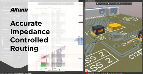
Altium has approached this problem by engineering the best layer stackup editor with an integrated PCB transmission line calculator. Transmission line impedance and dispersion need to be calculated when the layer stack is created so that design rules on trace widths in each layer can be created. Altium Designer includes these features and many more in an integrated layer stack manager and the industry's best routing features. Anytime you create a design in Altium Designer, you'll know that impedance is calculated accurately and your routing will meet impedance and loss targets.
ALTIUM DESIGNER
PCB design software with a transmission line calculator for high-speed/high-frequency designs and the industry's best routing utilities.
High-speed and high-frequency designs require an impedance controlled design approach, where the width of traces is set to a specific value so that transmission lines have a specific impedance. The impedance is related to the propagation delay in your transmission lines, which will determine the constraints set on length matching in the PCB layout. Finally, losses are also related to the impedance in your transmission lines, so designers need the best PCB transmission line calculator to ensure their PCB trace width will accurately determine the impedance and other signal integrity characteristics.
While an online PCB transmission line calculator can give you a lossless design calculation, the impedance of real transmission lines cannot be determined accurately with these free design tools. Your PCB design software should include these features as built-in tools to help you produce an accurate PCB layout.
Factors Determining Transmission Line Impedance
Impedance of transmission lines is determined when the layer stackup for your design is created. Having the ability to change the following board layer attributes gives you control over your impedance, losses, and propagation delay during routing:
- Real part of the dielectric constant
- Loss tangent and dispersion
- Distance between the trace and the nearby reference plane
- Copper trace thickness and roughness
- Trace width
When designing a PCB stackup, the designer needs to set the layer arrangement and layer thicknesses, and they need to select materials for their PCB. Once these decisions are made, a designer needs to determine the PCB trace width required to hit their required PCB transmission line impedance. Online calculators will generally use Wadell's equations to determine the transmission line impedance numerically. Simpler calculators will use the less-accurate IPC-2141 equations. A PCB transmission line calculator you'll find online or in many design applications can't be used to get accurate impedance values because they do not include a consideration for loss tangent or dispersion in these calculations. Therefore, a more accurate utility is needed for these tasks.
Use Altium Designer for Stackup Design and Impedance Calculation
Altium Designer's PCB stackup editor lets you setup the layer stack you need for your design, and you can run impedance calculations for your trace arrangement as you design your PCB. The impedance profile you calculate for your PCB traces on each layer will include considerations for dispersion, losses, and copper roughness. This is by far the simplest and most powerful PCB transmission line calculator you can use to design your stackup and determine the required trace width in your design.
- Copper roughness effectively increases the skin resistance of your traces and thus increases the total impedance until you reach very high frequencies.
Learn more about the important of copper roughness and how it is modeled. - All PCB interconnects that require impedance control need to have a ground plane below the trace layer to ensure consistent impedance.
Learn more about defining a ground plane in Altium Designer. - The layer stack manager in Altium Designer gives you control over many important functions, including setting layer arrangements, defining drill pairs and vias, setting up flex regions for a rigid-flex board, and backdrilling. Use the Impedance tab to start your PCB impedance calculation for different layers.
Learn more about stackup design in Altium Designer.

How to Use PCB Trace Width Calculations
The width of traces has a direct impact on the ability for a transmission line to maintain consistent impedance, and the width needs to be enforced on a trace no matter where the trace is routed. Trace widths need to be determined on each layer and enforced on a specific net as a design rule. Once you determine the PCB trace width required to reach you impedance target, it should be set as a design rule on the required net so that signal integrity can be maintained in the design.
Wider traces will have lower inductance, so they can receive less inductive crosstalk from nearby aggressor traces when routed along different layers in the PCB. If you're working with a dense design, or you are having problems with crosstalk in a design, you can set the design rule for your interconnects using a slightly wider trace. Altium Designer allows you to select the appropriate design rules for your interconnects and assign them to specific nets so that your transmission lines are routed correctly on any layer.
Interactive Routing of Transmission Lines in Altium Designer
The interactive routing features in Altium Designer can help you automate some of the basic aspects of routing, but they allow you to maintain control over routing paths and locations. The routing engine in Altium Designer enforces trace width limits, trace length limits, constraints on trace spacing, and deviation from ground planes when routing in the PCB. The results from your PCB transmission line calculator are used by the routing engine to enforce these limits so that you won't have to manually track and adjust trace geometries throughout your PCB layout.
- Altium Designer's high-quality design rules engine integrates with routing features to help you place and route traces and components in your PCB layout accurately.
Learn more about setting design rules for routing your PCB. - The propagation delay you determine from your PCB transmission line calculator can be used for length matching using your routing features.
Learn more about length matching structures for high-speed signals in PCB traces. - Altium Designer's layer stackup editor and PCB transmission line calculator use an integrated 3D field solver to produce accurate calculations as you start to create your design.
Learn more about Simberian's 3D field solver in Altium Designer.

PCB Layout Verification and Simulation in Altium Designer
The layout and routing tools in Altium Designer include a signal integrity engine that interfaces with your design rules to help ensure your signal behavior complies with limits on signal distortion and losses. Crosstalk, reflection, termination, overshoot, and skew can be evaluated for high-speed signals within Altium Designer to help verify transmission line designs. In addition to these built-in features, the extensions in Altium Designer allow users to access 3rd party applications for simulating EMI, power integrity, noise, thermal behavior, and much more.
A Comprehensive Toolset for High-Speed PCB Design
Altium Designer includes the industry's best routing engine with an integrated link to your design rules, but the software can do much more than help you route your traces. Altium Designer users have access to a huge library of components, a complete set of manufacturing tools, CAD features to create innovative layouts, and much more. You can also create and simulate your high-speed designs with impedance-controlled transmission lines using built-in tools in Altium Designer, or using 3rd party applications. Use Altium Designer to keep yourself at the cutting edge with a complete set of layout and routing features for advanced electronics.
- With the complete set of PCB design features in Altium Designer, you'll have the tools you need to create advanced electronics and for any application.
Learn more about the PCB design tools in Altium Designer. - Once your impedance profile has been determined, your PCB trace width calculation can be implemented as a design rule in your routing tools. Altium Designer's interactive routing features set the standard for high-speed and high-frequency transmission line designs.
Learn more about the interactive routing features in Altium Designer. - All Altium Designer users can share their PCB designs through the Altium 365 platform. Design teams use Altium 365 to stay productive and share design data in a secure cloud environment.
Learn more about sharing your PCB design data on Altium 365.

The transmission line design and routing utilities in Altium Designer give you the complete package: an advanced calculator, a powerful routing engine, and an automated DRC system to help you stay compliant. The PCB editor in Altium Designer includes the industry's best CAD features in a unified design interface. You can stay at the cutting edge and build the best electronics designs with the complete set of design features in Altium Designer.
Altium Designer on Altium 365 delivers an unprecedented amount of integration to the electronics industry until now relegated to the world of software development, allowing designers to work from home and reach unprecedented levels of efficiency.
We have only scratched the surface of what is possible to do with Altium Designer on Altium 365. You can check the product page for a more in-depth feature description or one of the On-Demand Webinars.

About Author
Related Resources
Related Technical Documentation
Table of Contents
Design to Release, Without the Friction
- Keep reviews tied to the right version
- Reduce handoff confusion and rework
- Spot sourcing and release risk earlier
- Work solo, share when needed
Get Started
Thank you, you are now subscribed to updates.