


Importance of Signal Integrity for High-Speed Designs in Your ECAD Software

At a Glance
Your PCB design software can help you create boards to ensure signal integrity in high speed designs. Learn more about how Altium can help you.


High-speed PCB designs use digital components that have very fast edge rates in their output signals. These components are commonly called “high speed,” and the signals they source can experience significant degradation in standard PCB materials. Signal integrity for high-speed PCB designs is important for ensuring data can be passed between components on a PCB and to ensure signals can be interpreted by a receiver component. There is also the matter of best PCB layout practices to ensure low EMI emission from a PCB.
With the best PCB layout and routing tools, you can ensure your design maintains high-speed signal integrity with the best impedance calculators, interactive PCB routing features, and integration with powerful field solvers. Crosstalk and reflection simulations also help ensure your design meets basic performance standards and that your signals stay strong.
ALTIUM DESIGNER
A unified PCB design application with a complete PCB editor, signal integrity analysis features, and manufacturing tools for professional PCB designers.
When you’re working with high-speed signals and high-speed components in your PCB, signal integrity for high-speed designs should be top of mind. High-speed systems and the signals within them will experience signal integrity problems like excessive loss, signal distortion, and EMI that can create a major headache for a high-speed PCB designer.
When you need the right toolset for high-speed digital design, look no further than the best set of layout and routing features in Altium Designer. When you work with Altium’s flagship PCB design software, you’ll have a complete toolset for designing high-speed interconnects, performing signal integrity analysis, and much more. If you’ve never seen how your high-speed digital design tools can help you conquer signal integrity problems in your PCB, keep reading to learn more.
Importance of Signal Integrity for High-Speed Designs
Signal integrity problems sound esoteric, but all designs have them. It’s simply a question of whether they interfere with your components and prevent data reception. In the case of high-speed digital design, some basic measurements and signal integrity simulations can show when signals are experiencing excessive distortion. Some signal integrity problems you can identify in your high-speed PCB include:
- Excessive insertion loss in long channels
- Dominant reflection loss in short channels
- Dispersion, leading to spreading of digital signals and phase distortion
- Strong crosstalk, or ground bounce that mimics crosstalk
- Skew and jitter can only be identified with power integrity analysis
- Reflection at a receiver due to impedance mismatch
These problems lead to inter-symbol interference, creating high bit error rates due to unrecoverable signals. These problems occur in single-ended and differential channels, and designers should understand how their design features can help them confront and solve these problems in high-speed PCB designs.
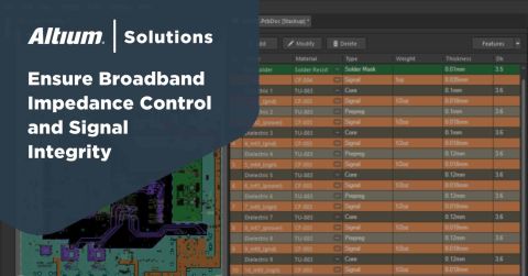
High-Speed PCB Design Starts With the Right Layer Stackup
Your PCB stackup should be designed correctly to ensure controlled impedance for high-speed interconnects. The layer stackup will also be a major factor that suppresses emission and reception of EMI. With Altium Designer’s PCB layer stack design features, you can build a solid foundation for your high-speed digital circuit board, no matter what frequencies or data rates are involved. In addition, you can route your transmission lines to ensure you meet target impedance goals up to very high-frequency values.
- Your PCB layer stackup design is one determinant of reliability. Be sure to pick the correct copper weight and dielectric PCB materials to ensure you satisfy your target impedance in your high-speed interconnects.
- When selecting core and prepreg, pay attention to material selection as dispersion is a major driver of signal integrity problems.
Learn more about dielectric dispersion in FR4 laminates and other substrates.
- Once you’ve created your stackup, you can define the target impedance you need to meet your high-speed digital signaling standards and ensure performance.
Learn more about designing to target impedance in the best PCB design software.

Instantly determine your required PCB trace width to meet your target impedance in Altium Designer.
Design Rules for a High-Speed Design Process
Creating a layer stackup is the first step to ensuring signal integrity for high-speed designs. However, much more needs to go into your PCB layout to prevent signal integrity problems. Many signal integrity problems originate from bad routing choices, but you can ensure your trace routing meets basic requirements with the best routing features.
Routing tools don’t need to be entirely manual. The best PCB routing features for high-speed circuit board design will use your target impedance as a design rule. As you create your PCB layout, you can instantly set target impedance tolerances for your high-speed interconnects, and the routing tools will help automate the layout process for complex PCBs. You’ll find these rules-driven design features and many more in Altium Designer.
Stay Productive With High-Speed PCB Design Rules in Altium Designer
The power of Altium Designer comes from its rules-driven PCB design engine. This powerful layout and routing engine will instantly check your circuit board layout against critical design rules as it’s created. You won’t have to manually run DRCs each time you layout a high-speed interconnect, and you won’t have to manually perform signal integrity analysis calculations to see if you’ll break your target impedance. Instead, everything you need to ensure signal integrity in high-speed designs happens as you work to help you stay productive.
- The routing engine in Altium Designer lets you instantly implement various routing styles to apply delay tuning and length matching in your high-speed interconnects.
- For differential pairs, each trace in the pair will need precise length matching to ensure signal integrity and common-mode noise rejection.
Learn more about differential pair length matching in Altium Designer.
- When you need to assess aspects like EMI performance, target impedance, and distortion in signal integrity analysis, Altium Designer users can import their PCBs into Ansys field solvers for powerful numerical simulations.
Learn more about performing high-speed signal integrity analysis in Ansys field solvers.

Take control over your high-speed digital design and signal integrity with a complete set of PCB layout tools in Altium Designer.
Interface With the Best Signal Integrity Analysis Tools
The importance of signal integrity for high-speed designs can’t be understated, and designers need a complete set of design tools to help them stay productive. Once you’ve finished your circuit board layout with the best CAD features and routing tools, you can use post-layout simulations to verify it against performance and reliability standards. These simulations include:
- Industry-standard IBIS model-based signal integrity simulations
- Crosstalk simulations across groups of high speed interconnects
- Reflection simulations to identify broadband impedance mismatch
- Interfacing with field solvers in Ansys software for network parameter and EMI simulations
Unlike other design programs, Altium Designer helps minimize the size of your software stack by giving you access to a range of design and simulation tools. Stay productive and design successfully with Altium Designer.
Take Advantage of Altium’s Extensive Signal Integrity Expertise
When you use Altium Designer, important signal integrity analysis tasks are easy thanks to a complete suite of tools for high-speed PCB design and analysis. Integrated simulators can help you perform important signal integrity analysis tasks and identify when your board will experience excessive losses, dispersion, distortion, and noise. Use the best high-speed signal integrity analysis features in Altium Designer to keep your system running at peak performance.
- Altium Designer’s complete set of PCB design and analysis features can help you conquer your high-speed PCB design projects and identify important signal integrity problems in your layout.
Learn more about the integrated design environment in Altium Designer.
- The PCB stackup design features and routing features in Altium Designer integrate with Simberian’s powerful 3D field solver, giving high-speed PCB designers accurate impedance and propagation delay calculations.
Learn more about Simberian’s integrated 3D field solver in Altium Designer.
- Altium 365 gives design teams a way to collaborate in a securely managed cloud environment. You can instantly share your design and production data through Altium Designer or on the web.

Use the best 2D and 3D PCB layout tools in Altium Designer to create your next high-speed digital circuit board.
Everything you need for circuit board design, layout, and manufacturing can be found in Altium Designer. You can take control over all aspects of signal integrity for high-speed designs with the complete set of PCB design tools in Altium Designer.
Altium Designer on Altium 365 delivers an unprecedented amount of integration to the electronics industry until now relegated to the world of software development, allowing designers to work from home and reach unprecedented levels of efficiency.
We have only scratched the surface of what is possible to do with Altium Designer on Altium 365. You can check the product page for a more in-depth feature description or one of the On-Demand Webinars.

About Author
Related Resources
Related Technical Documentation
Table of Contents
Design to Release, Without the Friction
- Keep reviews tied to the right version
- Reduce handoff confusion and rework
- Spot sourcing and release risk earlier
- Work solo, share when needed
Get Started
Thank you, you are now subscribed to updates.