What Ultra-HDI PCB Capabilities Can You Access?

When we talk about packaging, substrate-like PCBs, and fine-line PCBs, we are collectively referencing an area where PCB fabrication processing is pushing to the limit. This area is ultra-HDI, where the typical features in a PCB are scaled down to very small values. These more advanced capabilities enable traditional design practices with larger BGAs, but instead scaled into very fine pitches (0.3 mm) requiring tight spacing and linewidth.
These capabilities were historically available in Asia, and previously they only became really cost effective with volume production. Now that global access to these advanced capabilities is broadening, more designers can access these capabilities at lower volume, and even during prototyping. This also means more of the advanced components found in high-volume produced consumer devices can be used at lower volume.
Ultra-HDI Pushes Fabrication Capability Limits
Ultra-HDI is not a new approach to designing PCBs. The capability, whether subtractive or additive, has been available for very dense PCBs (such as in smartphones) and in IC packaging (in substrates and RDL). The capability was typically only cost effective when volumes were very high, which is why it has enabled some of the highest-compute consumer products and IC production with higher I/O counts. The capability is now becoming more accessible with lower volume fabricators.
The table below lists some of the fabrication features that are typically associated with ultra-HDI. These values were compiled from two different US manufacturers offering these capabilities. The feature limits listed below are not comprehensive; different manufacturers will provide different guarantees as to their ultra-HDI fabrication capabilities.
|
|
|
|
|
|
|
|
|
|
|
|
|
|
|
|
|
|
|
|
|
|
|
|
|
|
|
|
|
|
A couple of the capabilities listed above are typical for standard HDI boards, while others exceed the current standardization defined in IPC-2226 (Level C). For example, in these boards the through-hole via sizing limit is the same as in standard HDI. However, the linewidth limit is much smaller, down to 0.6 mils. Depending on the linewidth, etching may be possible but eventually an additive process would need to be used (e.g., SAP, mSAP, or A-SAP).
What Can You Do With Ultra-HDI?
Because ultra-HDI pushes feature sizes to low limits, the approach enables two design benefits:
- Layer reduction in an HDI board - Fine-line routing could enable consolidation of traces into smaller layer count, which reduces the number of HDI buildup layers.
- Small linewidths in conventional builds - If you can eliminate HDI buildups totally, you can greatly reduce the costs required to fabricate the PCB.
If you can reduce the number of HDI buildup layers, you can offset some of the additional costs required to access ultra-HDI fabrication capabilities.
Example 1: Xilinx FPGA (0.8 mm BGA)
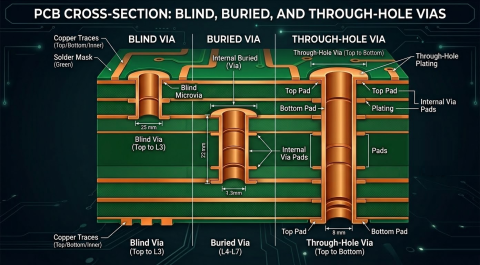
BGAs are often drivers of HDI fabrication due to the need to create the fanout for these large packages. This is typically done with stacked blind-buried mechanically drilled vias. At 1 mm pitch, you can typically use through-holes down to 8 or 10 mils depending on pad/ball size. Because of the pitch and linewidth limits, you might only be able to fit a single trace between balls in each layer.
With ultra-HDI capabilities, you could now fit two reasonably wide traces between pads. Depending on the pinout, this might allow for layer reduction because you can consolidate traces into a smaller number of layers. The image below shows a few traces in a DDR interface with trace width = 2.25 and S/W = 1.5.

Bringing traces closer in this way will increase crosstalk, but we can overcome this by using a thinner dielectric layer (smaller distance from traces to GND).
Because the crosstalk level is nonlinearly related to the layer thickness, a thinner layer will allow you to hit your impedance target and allows this denser routing without a huge crosstalk penalty. This generally means the thinner layer is required in these dense boards, especially when impedance is considered.
What if we were more aggressive and went with finer trace widths for the same S/W ratio? In the image below, I’ve reduced the trace width to 1 mil; with the same S/W ratio, we can now pack 4 traces between pads in this BGA. However, due to the challenge with crosstalk and the impedance requirement in a DDR interface, the design will require a thinner layer to ensure the trace impedance requirement is reached.

By doubling or quadrupling the number of traces passing between pads in the BGA footprint, we can potentially reduce the number of layers required to fully fanout the BGA. In smaller pitches (0.5 mm to 0.8 mm) that would typically require blind/buried vias and finer routing between pads, we could end up reducing the number of HDI buildup layers, which will significantly reduce the number of process steps and will help control fabrication costs. It might even be possible to convert an HDI build into a conventional build, which could offset the costs for fine-line fabrication.
Example 2: nRF52 WLCSP (0.35 mm BGA)
In very fine pitch components, the traditional approach is to use blind/buried vias and route underneath pads in each layer. There is simply no room to route between pads with traditional capabilities due to the clearance requirements between balls in the BGA. Ultra-HDI changes this by allowing both smaller vias and thinner traces, so the available routing area becomes limited by the pad size.
The routing example below shows our earlier nRF52 module project, but redesigned with fine-line routing between pads in the BGA fanout. In the original version of this project, the board was designed with a 2 + N + 2 stackup on 6 layers. With an ultra-HDI capability, I’m able to route between pads on a single layer. Here I’m showing two examples in the same image:
- 1.75 mil trace width with 1.75 mil spacing to pads
- 1 mil traces with 1 mil spacing (trace-to-pad and trace-to-trace)

With this BGA pitch, I can comfortably fit a 1.75 mil trace/spacing between two pads, or I can go more aggressive and fit two 1 mil traces between two pads. The first case is a better option due to the greater crosstalk between the traces in the 2x routing.
Obviously, the spacing between the 2x traces is less than the 3W rule limit. Can we violate this limit and still expect reasonable crosstalk? The answer is “maybe”... I’ve shown in other articles, and it is well-known among SI engineers, that bringing ground closer to a pair of traces reduces their mutual capacitance and inductance. Therefore, going to this more aggressive routing requires using thinner layers. This is because:
- The closer ground region reduces crosstalk for a given layer thickness
- For impedance controlled lines, the thinner layer allows a typical impedance target to be hit
This is why the 2x trace routing in this very fine pitch may not be the best option given the potential crosstalk between these traces. A better option is the 1.75 mil routing, and if this is done on a thicker layer (~3 mil) then any impedance controlled traces could still hit a 50 Ohm target.
Materials for Ultra-HDI
In the above discussion, I’ve gone pretty deep into materials needed for UHDI boards. There are two reasons for this that relate to signal integrity: crosstalk between closely spaced traces, and hitting impedance targets with narrow linewidths.
To achieve these goals with very thin traces, thin layer counts are required. Typically an upper limit of 50 microns is applied in a variety of possible materials, such as those listed in Happy Holden’s list of 11 HDI materials. Some common alternatives to laser-drillable materials and thin reinforced FR4 include:
- Ajinomoto build-up film (ABF)
- BT epoxy-based materials
- Thin liquid crystal polymer (e.g., UltraLam)
- Resin-coated copper films (metalized polyimide, pure polyimide, cast polyimide)
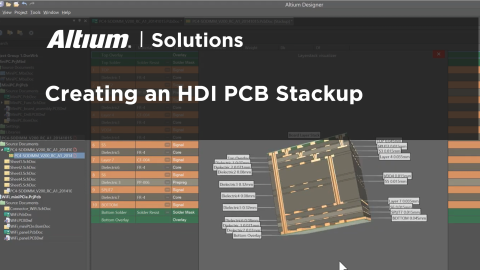
These may be used in combinations to create an ultra-HDI build. One such combination is the use of BT epoxy-based laminates as a core with conventional buried via, and ABF as the outer buildup layers that support fine-line routing. This buildup style is used as an organic substrate in BGA packaging, but the same approach can be used for an ultra-HDI PCB. An example of this build is shown below.

Higher Cost, But More Options
While these more advanced design practices carry higher fabrication costs, and they require a new approach to stackup design and routing, you can access more advanced components in fine pitches for your PCB. Overall, fine-line fabrication could reduce the number of HDI buildup layers required to work with these finer pitches by enabling routing between balls on fine-pitch BGAs.
In some cases, ultra-HDI can be a big cost reducer due to layer consolidation and conversion to a conventional mechanically-drilled through-hole build. If you can fit 4x traces between pads in BGA on 8 layers, that same board might require 32 layers if you could not access ultra-HDI capabilities. If you’re interested in these capabilities, they are just starting to become available in the US and Canada, and they can still be accessed in Europe and Japan.
Whenever you need to design an ultra-HDI PCB, make sure you use the complete set of PCB design features and world-class CAD tools in Altium Designer®. To implement collaboration in today’s cross-disciplinary environment, innovative companies are using the Altium 365™ platform to easily share design data and put projects into manufacturing.
We have only scratched the surface of what’s possible with Altium Designer on Altium 365. Start your free trial of Altium Designer + Altium 365 today.

