Differential Microstrip Impedance Calculator


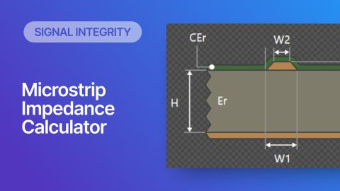
Are you looking for a free tool that you can use to calculate the impedance of differential microstrips? We created a simple tool you can use to calculate differential microstrip impedance for a given geometry and dielectric constant. If you’ve been looking for an accurate differential microstrip impedance calculator, then the calculator below is certainly one of the best free tools you’ll find on the internet before you start using field solvers to determine differential pair impedance.
Differential Microstrip Impedance Calculator
To use this differential pair impedance calculator, simply input your microstrip geometry and Dk value, and the tool will return the differential impedance value for a pair of microstrip traces. The calculator shown below uses Wadell’s equations for differential impedance, which can be found in the seminal textbook Transmission Line Design Handbook. These equations are rather complex, comprising a set of 67 interrelated equations and parameters, which includes a requirement to calculate elliptical integrals to solve these equations. The differential pair calculator below automates this for you, giving you the odd-mode impedance for a single trace and the differential impedance for the pair.

Results
To learn more about trace impedance calculators, Wadell’s equations, and some drawbacks of differential impedance calculators, read this article on single-ended microstrip impedance calculators.
When designing differential pairs and calculating their impedance, it’s important to understand how coupling will affect the pair. This is determined by the spacing between the pair as well as the width between the two traces. The single-ended impedance of each trace is important for termination, but the characteristic impedance is not the same as the single-ended impedance; the correct single-ended impedance is the odd-mode impedance listed above. Therefore, no matter how you plan to route your differential pairs, you should understand how coupling between the pairs creates deviations from characteristic impedance.
Drawbacks of Analytical Impedance Calculators
Differential impedance calculator tools are very useful for understanding how geometry affects the impedance of differential microstrips. However, there are many important pieces of information that are not included in a typical differential microstrip impedance calculator:
- Dispersion - The dielectric constant will be some function of frequency. The above value does not depend at all on frequency, but rather assumes a single frequency for a digital signal, which is incorrect. Learn More.
- Copper roughness - The roughness of copper foils used in PCB layer stacks adds some impedance by increasing the magnitude of the skin effect. Learn More.
- No dielectric losses - The above calculator also only takes the real portion of the dielectric constant as its input, but the loss tangent is omitted. Learn More.
- No etch factor - Etching causes the finished trace to have a trapezoidal shape, not a rectangular shape, which will cause the real trace to have a different impedance. Learn More.
- No propagation delay - Most online calculators shown above don’t give a propagation delay value, or if they do it’s estimated using a formula that is known to be incorrect. Learn More.
- Solder mask - The solder mask will modify the impedance and introduce additional losses along the transmission line, but online impedance calculators do not include these contributions. Learn More.
Use a Layer Stack Tool With a Built-in Field Solver
Simple differential pair and impedance calculator tools like the one shown here are very useful for estimating impedance, but the drawbacks listed above should reveal the inability of simpler impedance solvers to address advanced designs. Either you must manually apply corrections to a lossless model by adding back in the skin effect/roughness impedance, or you must solve Maxwell’s equations directly to get the impedance. The latter requires a field solver or a numerical model that is extracted from field solver results.
Altium Designer's PCB Layer Stack Manager includes a field solver that provides highly accurate impedance results. To access these features, simply open your layer stackup in the PCB Editor and click on the Impedance tab. From here you can create a design rule based on your impedance calculations, and this will enforce the calculated trace geometry as you route the PCB. The only thing you need to know to get started is the dielectric constant (real and complex parts) of your substrate materials.

The built-in layer stack editor in Altium Designer® can act as your own powerful differential microstrip impedance calculator, both for standard microstrips and coplanar arrangements. When you’re ready to release these files to your collaborators for more advanced simulations, Altium makes it easy to collaborate and share your projects. Everything you need to design and produce advanced electronics can be found in one software package.


