


Does Anyone Still Use DIP Components?

At a Glance
DIP components are less-often used in professional PCB design projects for new products, but legacy products may still need these parts.


Look around any electronics lab at a college or university, and you’re bound to find some dual inline package (DIP) components lying around. Electronics courses that have a lab component still overwhelmingly use DIP components. They are inexpensive, they can be easily mounted in breadboards without soldering, and they have common part numbers across vendors. Given these points, it makes sense that DIP components are so heavily used in educational settings and in hobbyist electronics kits.
Next, look at the professional electronics design and production space. Components are overwhelmingly surface-mount, and even if an IC is a through-hole component, it might not be in a DIP component. So this begs the question: is anyone still using DIP components in professional designs?
It might be surprising, but there are still DIP components that are widely used, they just do not support the newest technologies. Legacy technologies introduced decades ago still require maintenance, and these systems probably used a fair number of DIP components.
Why DIP Components Are Still Used
DIP components are well-known, and they are usually the first integrated circuits designers will interact with in their engineering courses. Many common parts are available as DIP components, including:
- Op-amps, comparators, and Schmitt triggers
- Small microcontrollers
- Memories (EEPROMs and Flash)
- Discrete semiconductors (e.g., diode arrays and MOSFETs)
- Gate drivers, LED drivers, or line drivers
- DC/DC converter controllers
- Optocouplers
- Relays
- Switches
- Resistor networks
Most semiconductor vendors will also make their components available in DIP components, and some of these are excellent drop-in replacements for each other across vendors. This is because they will have common pinouts and feature sets, as well as comparable prices.

DIP components still see widespread use in legacy and in new systems, including in mixed technology (SMD and through-hole) systems. Applications can be found in audio, high power systems, and high reliability systems. Older designs that have not been revised, but that still perform critical tasks, will continue to include DIP components due to the wide availability of these parts from multiple vendors.
Disadvantages of DIP Components
With so many options for DIP components, why aren’t all products still using DIP devices? There are several reasons for this, and most of them relate to a single factor: the size of DIP components. DIP components are very large compared to almost all SMD packages. In terms of I/O density, every SMD package has higher density; you can fit more pins (and thus signals) into a smaller space with SMD packages vs. DIP components.
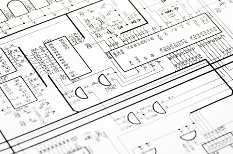
Consider the DIP-14 package shown below; the dimensions are listed in the drawing, and the component length is 1.9 cm. Suppose this package was a square shape with 7 pins lined up on each side; we would have a total of 28 pins. A QFN package with the same dimensions would have 192 pins around the edges, and a BGA package could have well over 1000 pins depending on its ball pitch. DIP packages simply can’t compete with these modern SMD packages in terms of I/O count and density.

The package itself also cannot support fast logic transitions that are required in modern computing protocols. This is because of package parasitics (pin-package and lead capacitance), which limit the available channel bandwidth and greatly slow down signal transitions. While it is true that two of the major drivers towards smaller electronics are feature density and cost, the other big factor is that performance increases (speed and power) come with smaller devices. This is another area where DIP components simply can’t compete.
Advantages of DIP Components
Although modern electronics simply wouldn’t function with DIP components, these parts do have their advantages. I’ve highlighted the main advantages above; they fall into four areas:
- Availability across multiple vendors
- Compatibility across multiple vendors
- Comparable cost to SMD ICs
- Very easy to place and solder by hand
These factors should illustrate why it can be so much easier to support an older system built with DIP components rather than rebuild an old system with the newest components. In some cases, parts of an old system fail and need repair; rework with DIP components in legacy systems is very easy and can often be done on-site. Some legacy systems still create millions of dollars in value and would be prohibitively expensive to reengineer, therefore it is often preferable to maintain older systems with DIP components rather than begin a total redesign.
Summary
Despite the fact that DIP components are older and do not make a strong appearance in new systems, they still enjoy widespread usage, particularly in support of legacy systems. They are also easily swapped if they fail in a legacy system, either by desoldering from a board or replacing them in a DIP socket. Based on these points, we shouldn’t expect DIP components to disappear anytime soon.
No matter what components you need to use in your designs, you can create schematic symbols and PCB footprints in seconds using Altium Designer®. The IPC Compliant Footprint Generator makes DIP component creation quick and easy, or DIP components can be quickly found in the Manufacturer Part Search Panel. Once you’ve found parts and created your libraries, you can easily share data and release files to your manufacturer with the Altium 365™ platform.
We have only scratched the surface of what’s possible with Altium Designer on Altium 365. Start your free trial of Altium Designer + Altium 365 today.

About Author
Related Resources
Related Technical Documentation
Table of Contents
Design to Release, Without the Friction
- Keep reviews tied to the right version
- Reduce handoff confusion and rework
- Spot sourcing and release risk earlier
- Work solo, share when needed
Get Started
Thank you, you are now subscribed to updates.


