


The High-Speed PCB Stackup Design Challenge

At a Glance
Stackups for high-speed PCBs can be designed many ways, but these systems must be built by balancing engineering constraints in a final product.


As much as we would like to build every high speed PCB perfectly, with ideal SI/PI/EMI characteristics, it isn’t always possible due to many practical constraints. Sometimes a stackup can be “good enough,” even for a high-speed PCB. This always comes from the need to balance engineering constraints, functional requirements, and the need to ensure signal and power integrity in a high-speed design, and finally to ensure compliance with EMC requirements.
Even with all the good guidelines out there for high speed design, there are particular aspects of stackup construction and their relation to building boards that get overlooked. My goal here is to go beyond just the typical SI/PI guidelines and look at these problems from more of an engineering perspective. When I say “engineering perspective,” I’m referring to all the other constraints in a product that drive the board design.
Translate Product Constraints into Stackup Needs
If we start from the engineering perspective, we should begin by developing a list of constraints and functional requirements for the system we want to build. In a high-speed PCB, we’re generally starting with a particular component we want to use. When working on client projects, this will almost always be a specific processor and its peripherals (CPU or FPGA, memories, other specialty chips, etc.). An example list of constraints that might apply in a typical high-speed PCB design include:
- Primary component pin count and lead size (e.g., BGA)
- I/O count in large components, which drives layer count
- Interface count, as well as the number of signals in each interface
- Board thickness target, which may or may not be standard thickness (62 mils)
- Loss target as compared to board size
Why start with this list? This is because the components being used reflect functional requirements, and the functional requirements will drive things like I/O count, and thus signal count. So before you start scanning through off-the-shelf materials, or before you start using a standard stackup, make sure you have some answers to the above questions.

Example board stack parameters for a 22-layer board with FR4 materials. With an FR4 core and prepreg set, your layer thickness can be larger, leading to a board thickness that is also quite large (about 3 mm in this case). Using alternative materials can give a thinner board and possibly reduce layer counts.
Now let’s try to mesh this list with the ideal high-speed PCB stackup and see if we can find convergence.
- Signal layers need to have adjacent ground layers to provide isolation
- Power layers need an adjacent ground layer
- If channels are very long, a low-loss material might be preferable
- Layer thicknesses might require a smaller via (blind or blind/buried) to hit I/Os
- You need specific linewidths and differential pair spacing to hit impedance targets
When we get to advanced boards with high layer count, we see the convergence between HDI materials and high-speed functionality. HDI stackups that require controlled impedance and support high speed interfaces will create challenges with linewidths and spacings, to the point that non-standard processing may be needed. The process below will go over the design challenges and should illustrate the DFM considerations that are needed in these products.
1. Start With Board and Layer Thicknesses
An important point to note in high-speed PCBs with high I/O counts is their layer thicknesses, which can be very thin. There is sometimes a misconception that going to very high I/O counts forces you to use a board that is larger than the standard thickness because the layer count becomes high. This is not necessarily the case; materials are available that can help designers stay at the standard board size target, but with low layer thicknesses.
The reason we care about layer thickness in a high-speed design is because it will determine the linewidth required to hit an impedance target. As a signal layer’s thickness scales lower, the required line width for impedance controlled signals also scales lower.
In the case where you’ve hit your limit on board thickness and you still need to get to thinner layer thickness, this may drive linewidths below the capabilities of a standard fabrication process or the HDI production process. Are there any materials that can be used to get to a smaller thickness without also reducing linewidth? The answer may lie in using a low-Dk material.
2. When Should You Use PTFE or Low-Dk Materials?
I can’t count the number of times a self-proclaimed guru has stated that low-Dk laminates or PTFE substrates should always be used in high-speed PCBs as a general rule. It’s important to remember that high-speed PCBs span a pretty wide range of possible data rates, edge rates, bandwidths, and trace widths. There are many designs that could be comfortably called “high-speed” but they aren’t built with a low-Dk laminate. Similarly, there are many high speed designs in the HDI realm that also use a low-Dk laminate, but it’s not always because they need to have low insertion loss.
Probably the most often-cited low-Dk material is ceramic-filled PTFE, which spans a huge range of possible materials. The Dk-value of PTFE-based materials is modulated through the addition of ceramic fillers, so a cured PTFE substrate could have a broad range of values. For example, PTFE materials could have Dk values ranging from approximately 3 to approximately 10, all with lower losses than standard FR4 laminates. You can view a selection of PTFE materials here.
|
|
|
|
|
|
|
|
|
|
|
|
|
|
|
|
|
|
|
|
The three main reasons to use a low-Dk material in advanced high-speed boards with thin signal layers are:
- Linewidths can be larger than on a high-Dk material for the same impedance target (See the graph above)
- If the material is unreinforced, there will be no skew from the fiber weave effect
- They can be available as thin laminates, so they can be used when layer counts are high
These three reasons illustrate why, when you get to high layer counts, the faster propagation delay in a low-Dk laminate is meaningless, contrary to the conventional wisdom. For professionals working in advanced boards, the linewidth issue will dominate, especially when designing high-layer count boards with controlled impedance striplines.

3. Balance Loss and Dk Value
When the layer thickness is small, the required linewidth needed to hit a particular impedance will also be small. If the linewidth is too small, then processing can be more challenging and costs will be driven up. Thus illustrates why point #1 above is important; lower Dk allows for wider linewidths for a given substrate thickness.
To balance low-loss and high-Dk, there are materials with Dk ranging from 3.5 to 4 with lower loss tangents than standard FR4; Rogers and Isola are two companies that produce these laminates, and I seem to recall another material available from ITEQ with loss tangent ~0.01.
If low-Dk is needed in a high-speed PCB at the HDI level, it will likely need to be glass-reinforced. This could be reinforced with spread glass at ~5 mils, but lower thickness may need a loose weave for reinforcement. The reinforcement with spread glass intends to minimize skew accumulation when the material is used for signal layers. The main reason for this is manufacturability:
- Unreinforced PTFE laminates are very flexible, especially in thin layers, to the point that they can be difficult to handle and place into a stackup.
- Because of #1, there could be some misregistration when building the layer stackup in standard processing.
4. If Low-Dk Isn’t Always Needed, Why Do RF Designers Use It?
PTFE laminates are a favorite among the RF community, and there are good reasons why we use it, but I don’t think digital designers know exactly why this is the case. The most commonly cited reason is the low loss value of some PTFE laminates and bondplies, such as RO3000 series materials.
One reason Dk values are carefully chosen in RF boards is to balance circuit size with loss. In fact, if you look at the PTFE laminate list above, you’ll see that some high-Dk PTFE laminates with lower losses than FR4 (just calculate the imaginary part of the dielectric constant). A higher Dk value provides smaller circuits at low frequencies (e.g., sub-GHz RF), but a lower Dk can help ensure something is manufacturable at high frequencies (e.g., radar).
|
|
|
|
|
|
|
|
|
|
|
|
|
|
|
The other reason a PTFE laminate would be used is because RF boards tend to have much longer channels in digital boards, so the dominating loss mechanisms will be related to propagation. These are the dielectric loss and the copper roughness loss. Today’s low-Dk PTFE materials have very low loss tangents, equating to low dielectric loss. These laminates can also accept VLP copper with very low roughness, so they can also offer lower copper losses than standard electrodeposited copper.
5. Embedded Capacitance Materials (ECM)
To aid power integrity, the dielectric that fills between power and ground plane pairs should be chosen correctly. The conventional wisdom around low-loss, low-Dk materials is wrong again here. The material used between a power/ground plane pair should not be a low-Dk material. Instead it should have a high Dk value and high losses. These layers should also be as thin as possible.
|
|
|
|
|
|
|
|
|
|
|
|
|
|
|
|
|
|
The industry has responded with very thin high-Dk materials that can be incorporated into resin-fiberglass systems. These embedded capacitance materials are not required for power integrity, but they are certainly helpful in high-speed PCBs with high layer counts. There are three reasons for this:
- High-Dk provides more plane capacitance
- Thinner ECM layers have more plane capacitance
- High loss in the ECM layer dampens power fluctuations very quickly
The Dk values of these materials can range from ~4 to ~10 from 100 MHz to 1 GHz. This is exactly the region where we would like to have plane capacitance that can dampen power plane resonances and any lack of on-chip/in-package capacitance. The thickness of these materials will be on the order of microns. Some companies producing these materials include 3M and DuPont; another well-known material is FaradFlex. Because these materials also have small layer thicknesses, they can be used in stackups with high layer counts.
Final Thoughts
In the high-speed PCB stackup design process, the act of building a PCB stackup is about the last step in the process. Instead we care much more about the layer counts and thicknesses in comparison to the component lead size and fanout. From there you can approach material selection for signal layers, and you can evaluate embedded capacitance materials for power/ground plane pairs.
If you’re just designing a simpler board, like a 4-layer board for high-speed, you really only have two things to determine: outer layer thickness and Dk value. Together these will determine the trace width you need to hit single-ended impedance, followed by spacing for a target differential impedance.
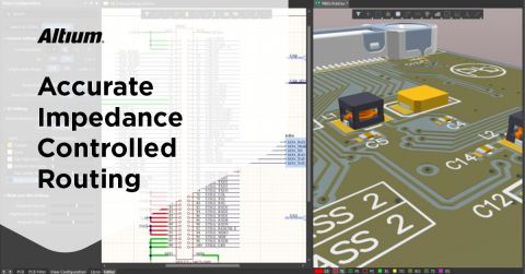
When you need to design your high-speed PCB stackup, use the complete set of PCB design tools in Altium Designer®. The Layer Stack Manager gives you full control over your PCB stackup, including material selection and impedance calculations. When you’ve finished your design, and you want to release files to your manufacturer, the Altium 365™ platform makes it easy to collaborate and share your projects.
We have only scratched the surface of what’s possible with Altium Designer on Altium 365. Start your free trial of Altium Designer + Altium 365 today.

About Author
Related Resources
Related Technical Documentation
Table of Contents
Design to Release, Without the Friction
- Keep reviews tied to the right version
- Reduce handoff confusion and rework
- Spot sourcing and release risk earlier
- Work solo, share when needed
Get Started
Thank you, you are now subscribed to updates.


