Why Most Via Impedance Calculators Are Inaccurate

At a Glance
Via impedance calculators are only useful in the low frequency range, where impedance control is typically not needed.


In my journeys through the land of LinkedIn, I’ve been seeing people post links to their via impedance calculators. Calculator applications are always nice to use for quick estimates of some aspect of a design, with stripline and microstrip dimensions being among the most common. For instance, I keep a skin effect resistance calculator in my toolbar so I can get quick estimates of copper-related losses in high-speed/RF interconnects.
The problem with every via impedance calculator that I have seen is simple: they are incomplete or totally wrong. The “incomplete” part refers to a lack of context; these calculators can roughly reproduce a well-known estimate from a legend like Howard Johnson in his Digital Design textbooks. However, these calculators never provide insight into what they are actually calculating, or where the calculated via impedance is accurate.
Ideally, you would like to design to a target impedance (usually 50 Ohms) when you have a high speed or RF signal you want to transfer through a via so as to minimize reflection. With high speed signals, where bandwidth is so large that the via appears very long at the signal’s Nyquist frequency, via impedance is now very important. However, most via impedance calculators get the results totally wrong in these frequency ranges as they do not consider wave propagation along the via structure. The value they actually give is only valid at very low frequencies, which is where you do not need to worry about via impedance.
Keep reading to see why these calculators get it so wrong, as well as the context surrounding via impedance.
*Note: Some results from 3rd party simulation products are shown below. These calculations are shown for educational purposes only. My mention of these products below does not constitute an official endorsement by myself or Altium.
What Via Impedance Calculators Are Actually Doing
A via impedance calculator you’ll find online will use a simple approximation for a lumped circuit model to calculate impedance. These models attempt to treat the via as a lumped element model for a transmission line with known inductance and capacitance. Those values can then be used to determine an impedance and propagation delay for the via structure.
A simple model for via impedance that is commonly used is the LC model. This model assumes the via barrel passes through a single antipad; the capacitance and inductance are then modeled based on the dimensions of the via, the top and bottom pads, and the antipad.
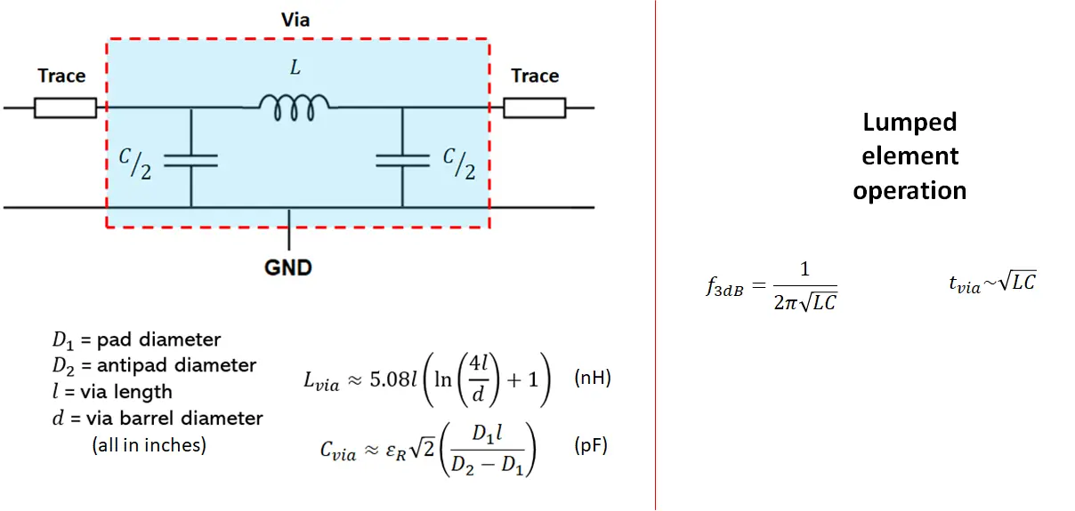
An LC filter model that can be used to calculate via impedance. Read more about this model in this article.
One thing these via calculators will tell you is that the typical 10 mil via/20 mil pad on Dk = 4 substrates has an impedance of about 50 below about 1 GHz, as long as you do not make the antipad excessively large. That is all fine, but at those frequency ranges, does the via impedance really matter?
Unfortunately, results from this model or similar models will most likely be wrong in frequency ranges where the via impedance actually matters for losses and reflections. Even if one of these via impedance calculators implements the LC model, that model is incomplete and will only be valid at very low frequencies. The reason is simple: you are attempting to use a lumped element model to describe impedance seen during wave propagation. As I’ve detailed in many other articles, this will never produce accurate results.
Real Vias Are Resonators
In ranges where a via would be used to support high speed or high frequency, the via and its nearby stitching vias must be treated as a cavity in which waves are propagating. At certain frequencies, the injected signal can excite some resonances, which will produce a standing wave pattern in the cylindrical structure, similar to what you would observe from non-TEM modes in a coaxial cable.
Clearly, a simple lumped LC model can’t possibly describe wave propagation. In addition to this fact, there are some other reasons that reveal why such models are incorrect and will not describe via impedance correctly.
How To Know When Via Impedance Calculators Give Wrong Results
There are a few things that tell me immediately that the current set of online via impedance calculators give incorrect results.
The result has no frequency dependence. Via structures are resonators like any other closed or semi-closed cavity, so they will have some resonances at different frequencies corresponding to the eigenmodes of the semi-coaxial via structure. Even an individual via with no stitching vias will have a set of resonances; these just happen to be scattering resonances and not closed-cavity resonances. Therefore, there will be specific frequencies where the electric or magnetic fields will have maximum or minimum values, respectively, as described above.
One way to see the effects of resonances is in the S-parameters (both S11 and S21). The graph and overlaid geometry below show an example of S-parameter values for a via design targeting a 68 GHz application. If these simple calculators were correct, we would have a flat S11 line, we would not see the very strong transmission peak with high Q value right at 68.2 GHz.

They don’t consider stitching vias. In the frequency range where via impedance is important, stitching vias are needed to set the impedance to the target value. The geometry of the stitching vias, their arrangement, and the antipad size around the central signal via is much more important to setting the impedance than just the signal via geometry. The impedance of the structure is also very sensitive to changes in these parameters.
The result is that the impedance will vary with frequency simply due to the geometry of the structure. This is a basic fact for any resonator or scatterer. In the case of a single via with no stitching vias, the impedance first appears inductive as we would expect, then it begins to appear capacitive as the low impedance between the pad/sidewalls and plane take over.

Now consider what happens when we add stitching vias around the structure. An example of a single-ended via with stitching vias and its frequency response is shown below. As we can see from this graph, the impedance is only constant at the target value at very low frequencies, and this only persists up to a couple of GHz. Beyond that, the impedance can first become inductive and then later can become capacitive in the mmWave range.

The fact that any of the simple via impedance calculators can’t account for this frequency dependence should illustrate that such results will only be useful at low frequencies.
It is known that simple via impedance models are incomplete. I bring this up because it is well-known that simple LC models and similar models are incorrect, and yet I am still seeing via impedance calculators that implement these models as if they are universally accurate and with no context given.
If you read Howard Johnson’s textbooks, in the section where he talks about signal propagation through vias, you’ll find that the author states the limits of the LC model for via impedance. To quote Howard Johnson:
|
|
- Page 342 in: Howard W. Johnson, and Martin Graham. High-speed Signal Propagation: Advanced Black Magic. Prentice Hall Professional, 2003.
In other words, the pi model and its less-accurate first-order variations are only valid in ranges where the via is electrically short and would be relatively invisible to a propagating signal.
These calculators do not give the correct propagation delay for a through-hole via. We should expect a through-hole via in standard thickness boards to have a total propagation delay ranging from 10-20 ps, depending on via dimensions and material constants. The simple online calculators you’ll find will tell you the propagation delay is always about 10 ps.
This is because, along the length of a through-hole via, the dielectric constant that determines signal propagation is an effective dielectric constant with value of ~14 when Dk = 4. Even Howard Johnson's original estimate of ~40 ps looks too large and it would predict an effective Dk of ~67. That's pretty large. Even in differential vias without surrounding stitching vias, the effective dielectric constant is not equal to the substrate Dk value, it is anywhere from 8 to 10.
The point here is that the effective Dk value that determines the signal behavior will be larger than the board material's Dk value. The online calculators I have seen do not account for any of this this and they will give wrong propagation delay results anywhere above about 3 GHz.
Don’t Forget: High Speed Vias Are Differential!
As soon as someone states “I need a via impedance calculator for my high-speed signals”, they probably forgot that those high-speed signals are most likely on a differential pair, so what you really need is a differential via impedance calculator, or rather an odd-mode via impedance calculator. The impedance of a differential via pair cannot be treated with a single via impedance calculator unless the vias are spaced far apart. This is the same reason we have to consider spacing between traces in differential pairs: the two conductors interact with each other to determine the odd-mode (and differential) impedance.

Don’t Forget: Digital Signals Are Wideband!
Remember that digital signals are wideband, with frequency content spanning well into the range where vias do not have a flat impedance spectrum. For digital signals with very short rise/fall times, significant power can be concentrated in ranges where the impedance is non-constant with frequency.
As a result, digital designers that must route through a via (or pair of differential vias) must design vias such that the deviation in the impedance spectrum is much larger than the bandwidth limit. They can do this principally with a few levers:
- Adjusting the anti-pad size
- Adjusting the pad size
- Adjusting the stitching via count and size
Microwave engineers once again have it easy when it comes to via design: they only need to design to a specific bandwidth around the carrier frequency for their signals. All other frequencies on a given interconnect are irrelevant. It’s often stated that vias must be avoided on RF interconnects, but the reality is that these are often needed for signal launch coming out of a connector, or to route into dense antenna arrays (e.g., in high-resolution MIMO imaging applications).
Based on these points, Howard Johnson arrives to the same conclusion I’ve arrived at here:
|
|
- Page 343 in: Howard W. Johnson, and Martin Graham. High-speed Signal Propagation: Advanced Black Magic. Prentice Hall Professional, 2003.
3rd Party Tools for Via Impedance Calculations
Calculating via impedance in the frequency ranges where propagation is evident is not for the faint of heart. If you want to calculate a general solution for the electric and magnetic fields in a via structure with stitching vias, it is possible to do it by hand using cylindrical Hankel functions. However, once you attempt to apply boundary conditions with thin conductive planes in the antipad region to get the particular solution to the wave equation in the via structure, the results can be very complex depending on the shape and size of the antipad.
Therefore, for the designer who is not a fan of these mathematical exercises, there are external tools you can use to simulate signal propagation through a via and extract the impedance. Some examples include:
- Ansys HFSS
- Simbeor
- COMSOL
- Simulia (CST)
These tools will implement a numerical routine to solve Maxwell’s equations (really the wave equation) in the via structure of interest. First the system is discretized, and an iterative numerical algorithm is used to calculate the electric and magnetic fields.

All of these can give you a via impedance, and they each have their merits and use cases. I like Ansys HFSS for this problem because I normally am doing this alongside an antenna simulation. In the RF designs I work on, the end goal is not the via impedance, it’s S11, an antenna gain, and a radiation pattern. CST can give you the same results, but it has much better model handling of multilayer boards with antipads when you do your STEP or Parasolid model imports into the simulator. COMSOL can technically do anything, but you'll need a Ph.D. in computational electromagnetics and hours of training to create this simulation.
If all you need to determine is the via impedance and S-parameters, Simbeor will complete the simulation results much faster than other applications. It has a tool specifically for vias, which you can use to include stitching vias and extract S-parameters. However, there are things that RF designers would need which can’t be done in Simbeor. Consider all of these points carefully before using an external simulation tool for these types of design problems, and make sure your simulation tool can support your model exports from your PCB design software.
Once you’ve qualified your design with a via impedance calculator, use the PCB layout and routing features in Altium to place and route your high-speed/high-frequency signals in your PCB. When you’ve finished your design, and you want to release files to your manufacturer, Altium makes it easy to collaborate and share your projects.

About Author
Related Resources


Related Technical Documentation

Table of Contents
Get the Full Signal Analyzer Experience
- Turn SI analysis into fast, coordinated decisions.
- Your Agile Teams evaluation includes full access to Signal Analyzer.
Contact Us
Thank you, you are now subscribed to updates.

