


PCB and Package Design for 224G PAM-4 Channels

At a Glance
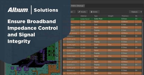
The next interface and packaging milestone is here with 224G PAM-4. Here is how these channels can be designed to provide broadband signal integrity.


As of 2023 and 2024, the next data rate doubling in data center architecture is taking us to 224 Gbps per lane of serial data. This data rate doubling is not achieved by doubling the clock directly, but rather by doubling the baud rate through higher order 4-level pulse amplitude modulation (PAM-4). The decision to implement PAM-4 is necessary in order to extend data rates without extending the required channel bandwidths
We are witnessing an interesting time in the development of high-speed serial links where binary RZ/NRZ signaling is no longer useful for transmitting digital data beyond 112 Gbps data rates. The use of 112G RZ/NRZ signaling requires 56 GHz of bandwidth, and doubling the clock at this rate would require doubling the bandwidth beyond what a PCB and package can support. The PCB interconnect and package interconnects are the two major bandwidth limiting factors in high-speed serial links.
Now, if you suddenly find yourself or your company working with 224G channels on a PCB or in packaging, this article will show you what these channels look like, both physically and in terms of signal integrity. By the end of this article, you'll also understand why we've reached a limit where we can no longer simply increase clock rates in order to get to hire data rates.
Broadband Channel Design at 56 GHz
The current class of 224G products being developed use PAM-4, or bit streams with four signal levels. This is equivalent to two bits per unit interval (UI) being transmitted along an interconnect. This sets the required channel bandwidth and receiver bandwidth to at least 56 GHz as measured in terms of return loss and insertion loss.

The entire goal of channel design in a PCB is to maintain TEM mode propagation up to the highest possible frequencies, at least exceeding the Nyquist frequency of 56 GHz. A related goal is to ensure lowest possible group delay dispersion as this will minimize phase distortion and minimize signal edge rate distortion. When using low Dk/Df substrate materials, there are three major bandwidth limiting factors at high frequencies.
- Excitation of non-TEM modes - determined by Dk and geometry
- Impedance mismatch due to inductance from copper roughness - determined by geometry and copper
- Excessive group delay dispersion - caused by variance in Dk as a function of frequency
For the vast majority of interfaces, you won't need to worry about non-TEM mode propagation in most PCBs. This is because non-TEM mode propagation does not begin until roughly 50-100 GHz anyways, depending on the geometry of the transmission line and the Dk value of the substrate. It is not until only recently that the digital world has had to deal with this challenge just as we have seen in the RF world.
Why do we care about TEM versus non-TEM mode propagation? The reason is that, at some high frequency, the first TE or TM mode will be excited by a broadband signal. Right at that frequency, there is a big impedance discontinuity as the new mode is excited and can begin propagating along the transmission line. This big impedance discontinuity right at the frequency corresponding to TE or TM mode excitation is a major bandwidth limiting effect at 56 GHz. This is why 56 GHz transmission lines are generally HDI and will use smaller width and dielectric thickness.

When designing a broadband TEM transmission line, we could use several signal Integrity metrics to characterize its performance over a broad bandwidth. Generally, these include (in order of importance):
- Return loss and insertion loss
- Impulse response
- Eye diagram and BER
- COM and ILD
Generally, the first place you start to look at channel compliance is with S-parameters. Desirable S-parameters for a channel up to 56 GHz are shown below. Here we prefer to have sub -10 dB return loss at all frequencies up to at least 56 GHz. Corresponding low loss is also desirable on in an IC substrate/package.

This level of qualification for a high-speed digital channel is generally required anywhere above approximately 3 to 5 GHz. Due to the length scales in PCBs and packages, this is the frequency range where small structures like pads, vias, and balls on a BGA start to create noticeable deviations in input impedance.
Now that we know the design requirements, let's look at the various factors that influence packages and PCBs designed to provide at least 56 GHz bandwidth.
Where Does Stuff Get Placed?
224G architectures with serial links require close placement between elements. In the package, things are obviously very close together. On the PCB, we have three possible architectures that can be used.

The more lossy the package and channel are on the PCB, the closer your receiving package must be to the transmitting package. Components are most often appearing as near-chip or on-package modules in order to complete the required interconnects. Putting these elements closer together allows you to reduce the total insertion loss, but it then causes the channel to be returned loss dominated.
In order to keep a system return loss dominated, materials and the vertical transitions are the main problems, although most people don't really understand why. At these frequencies the materials do matter because of insertion loss, and this is one reason we have an interplay between Dk, copper roughness, and trace length.
Trace Length, Dk, and Copper Roughness
Low Dk values for the PCB laminate or package substrate material are essential for two reasons:
- They allow for wider traces on thinner layers
- Low Dk increases the TEM cutoff frequency in a given geometry
The first point reduces skin effect, which then extends the bandwidth. It also reduces differential crosstalk. To see simulation data supporting these results, take a look at the other article on differential crosstalk. I calculate both quantities in the set of graphs in this article and I've summarized the effects in the table below.
Copper roughness arises as a bandwidth limiting factor in two ways:
- On low loss tangent laminates, copper roughness is the dominant loss mechanism
- Copper roughness creates an inductive addition to the impedance that increases with frequency
Both effects cause interconnects in a package and on a PCB to be required to be rather short. The second effect is one of the major reasons that transmission line impedance matching is very difficult at very high frequencies in the 56 GHz range, with the other factor being parasitics in the Tx or Rx package/buffer.
So clearly, we would prefer lower Dk and smoother copper. Lower Dk allows for thinner layers with wider traces, so it helps overcome copper loss. This then reduces the inductive contribution to impedance due to the skin effect, and it helps extend the bandwidth limit seen in the return loss spectrum. It also increases the frequencies corresponding to cylindrical resonances in via transitions, which extends TEM bandwidth in BGA packaging and on the PCB. This is the major reason lower Dk is desired at higher frequencies.
Loss Factors When Return Loss Dominates
When return loss dominates, we essentially need to remove any of the elements that create impedance mismatch along the interconnect, as was described above with smoother copper and lower Dk value. In both packages and PCBs, a major return loss factor is vertical transitions through vias. PCBs and packages use vias for vertical transitions. A package just uses vertical transitions as part of a bump-to-ball interconnect, eventually reaching the ballout on the bottom side of the BGA package.

If we just look at the above mesh for a differential via traversing from a package into a PCB, we can already pick out many possible parameters that need to be included and optimized in a given design. If we write out a list, we would have the following:
- Drill diameter of the via
- Length of the via
- Pad diameter
- Antipad diameter
- Number of layers traversed in the transition
- Via style (blind, buried, through hole, skip vias)
- Dk and Df values of the dielectrics
- Thickness of each layer
- Number of stitching vias and their locations
This is a huge list of parameters compared to the three parameters used to design a transmission line. This is one of the reasons that broadband via design is so difficult at very high frequencies. In comparison, transmission lines are quite easy to design, even up to 56 GHz bandwidths.
Transmission Line Options at 56 GHz
When working at 56 GHz with digital signals, the type of routing matters greatly. The designer needs to select whether traces will be routed in microstrip, stripline, or coplanar waveguide configuration. In a PCB, any of these are available for practical purposes. In packages, we more often see differential coplanar stripline waveguide configuration, which is known as skip-layer routing.
The table below illustrates the different options for differential pair routing in PCB and packages. Recall that we are working with return loss dominated channels, and routing tends to be dense, making crosstalk a big concern. The options below show various advantages in terms of skin effect impedance contribution and crosstalk.
|
Embedded microstrip |
|
|
Standard microstrip |
|
|
Coaxial stripline |
|
|
Coplanar waveguide |
|
The table above compares the various options that you will see both in packages and PCBs. The use of differential coplanar waveguides (both in microstrip and stripline) creates a kind of coaxial waveguide, which can have very high bandwidth. This fusion between coplanar waveguide routing and differential stripline routing is called skip-layer routing.
How to Create Skip-Layer Routing
The cross-sectional view of skip layer routing is shown below. Skip layer routing uses three options as indicated in the three panels in the figure. The common characteristic in this style of routing is the via fence placed along the differential pair.

An overhead view as shown below gives the general spacing conditions on the via fence along the differential striplines. This is the same type of spacing condition you will see for a single-ended coplanar waveguide for an RF interconnect. By placing the via spacing and pitch close together, the structure approximates a differential coax structure.

The other reason for the via fence is to confine the electromagnetic field around a differential pair and thereby reduce differential crosstalk. The data below shows that the staggered skip-layer routing arrangements have the lowest differential crosstalk. By staggering on two different layers, you are increasing the spacing between the differential pairs, which provides lower differential crosstalk.

The above illustrates the package styles used in 112G and 224G interconnects inside IC substrates. But when you need to design a PCB that also supports broadband signal transmission at these high frequencies, the above routing styles are also appropriate. In fact, we like to use stripline routing anyways due to FEXT suppression, so it makes sense to also use skip-layer routing with striplines.
Layer Transitions at 224G PAM-4
Vertical transitions through vias are challenging for the reasons I mentioned above. Not only is impedance design challenging, but the vias must also be designed to maintain TEM propagation vertically along the layer transition. This is yet another reason that we prefer HDI designs with tight spacing.
The data below shows the approximate TEM cutoff frequency in an IC substrate as a function of ball pitch in a BGA package. As we can see, TEM propagation ends and a higher order mode is excited at 59 GHz in a 0.8 mm pitch package, essentially leaving no margin of safety for 56 GHz channels. This is why we prefer to have smaller ball pitch: this will increase the cutoff frequency for TEM mode propagation.

There are some designers who are more experienced than myself who will say that stitching vias are meaningless on differential pairs and that the need for stitching via is a myth. Here, stitching visas are absolutely needed on differential pairs, but the reason is not simply to provide some return path. The reason is because it guarantees TEM mode propagation up to progressively higher frequencies. When the ball pitch and thus the stitching via pitch is smaller, the TEM mode cutoff is higher. Packaging designers have known this for many years, but the old guard of high-speed PCB experts does not seem to understand this fact.

Just as we had previously for stitching vias around our skip-layer routing, we have the same thing on the underside of our BGA package. The reason is that it also reduces differential crosstalk within the TM bandwidth limit. This is another point that the older high-speed designers will say is bogus, but the VPX backplane design world has known this for many years. Package designers also understand this fact and they implement it in ballout designs.
More Advanced Modulation Is Key to Higher Bandwidths
Above 28 GHz Nyquist, or in practical terms, above 56 Gbps NRZ/RZ signaling, TEM cutoff and roughness are the main bandwidth limiting factors. The industry is working towards sub-Dk = 3 materials with very low layer thicknesses, as well as more advanced processing, which will enable higher TEM cutoffs in packages and PCBs. However, the copper roughness issue still remains and it will not simply be possible to just double clock rates to double data rates.
Therefore, I expect that the next data rate doubling will require moving to more advanced PAM with >4 signal levels. For example, with PAM-8, you would transport 3 bits per UI, and the Nyquist frequency in a 448G channel would be 74.67 GHz. This type of higher order modulation may be the key to the next data rate doubling; for example, PAM-16 would enable a 4-bit per UI data rate doubling and would enable 448G data transmission with only 56 GHz bandwidth, but with highly compressed noise margin.

No matter what technology ends up enabling the next data rate doubling, PCB designers and packaging designers can create these systems and much more with the advanced design features in Altium Designer®. To implement collaboration in today’s cross-disciplinary environment, innovative companies are using the Altium 365™ platform to easily share design data and put projects into manufacturing.
We have only scratched the surface of what’s possible with Altium Designer on Altium 365. Start your free trial of Altium Designer + Altium 365 today.

About Author
Related Resources
Related Technical Documentation
Table of Contents
Design to Release, Without the Friction
- Keep reviews tied to the right version
- Reduce handoff confusion and rework
- Spot sourcing and release risk earlier
- Work solo, share when needed
Get Started
Thank you, you are now subscribed to updates.

